IRFBC30ASPBF Vishay, IRFBC30ASPBF Datasheet - Page 7
IRFBC30ASPBF
Manufacturer Part Number
IRFBC30ASPBF
Description
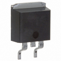
MOSFET N-CH 600V 3.6A D2PAK
Manufacturer
Vishay
Datasheet
1.IRFBC30ASPBF.pdf
(8 pages)
Specifications of IRFBC30ASPBF
Transistor Polarity
N-Channel
Fet Type
MOSFET N-Channel, Metal Oxide
Fet Feature
Standard
Rds On (max) @ Id, Vgs
2.2 Ohm @ 2.2A, 10V
Drain To Source Voltage (vdss)
600V
Current - Continuous Drain (id) @ 25° C
3.6A
Vgs(th) (max) @ Id
4.5V @ 250µA
Gate Charge (qg) @ Vgs
23nC @ 10V
Input Capacitance (ciss) @ Vds
510pF @ 25V
Power - Max
74W
Mounting Type
Surface Mount
Package / Case
D²Pak, TO-263 (2 leads + tab)
Minimum Operating Temperature
- 55 C
Configuration
Single
Resistance Drain-source Rds (on)
2.2 Ohm @ 10 V
Drain-source Breakdown Voltage
600 V
Gate-source Breakdown Voltage
+/- 30 V
Continuous Drain Current
3.6 A
Power Dissipation
74000 mW
Maximum Operating Temperature
+ 150 C
Mounting Style
SMD/SMT
Continuous Drain Current Id
3.6A
Drain Source Voltage Vds
600V
On Resistance Rds(on)
2.2ohm
Rds(on) Test Voltage Vgs
10V
Threshold Voltage Vgs Typ
4.5V
Lead Free Status / RoHS Status
Lead free / RoHS Compliant
Lead Free Status / RoHS Status
Lead free / RoHS Compliant, Lead free / RoHS Compliant
Other names
*IRFBC30ASPBF
Available stocks
Company
Part Number
Manufacturer
Quantity
Price


Vishay Siliconix maintains worldwide manufacturing capability. Products may be manufactured at one of several qualified locations. Reliability data for Silicon
Technology and Package Reliability represent a composite of all qualified locations. For related documents such as package/tape drawings, part marking, and
reliability data, see www.vishay.com/ppg?91109.
Document Number: 91109
S10-2433-Rev. B, 25-Oct-10
Re-applied
voltage
Reverse
recovery
current
IRFBC30AS, SiHFBC30AS, IRFBC30AL, SiHFBC30AL
+
R
-
g
D.U.T.
Note
a. V
Driver gate drive
D.U.T. l
D.U.T. V
Inductor current
GS
= 5 V for logic level devices
P.W.
SD
DS
waveform
waveform
Peak Diode Recovery dV/dt Test Circuit
Ripple ≤ 5 %
Body diode forward drop
Period
Body diode forward
-
+
Fig. 14 - For N-Channel
• dV/dt controlled by R
• Driver same type as D.U.T.
• I
• D.U.T. - device under test
Diode recovery
SD
current
controlled by duty factor “D”
Circuit layout considerations
dV/dt
• Low stray inductance
• Ground plane
• Low leakage inductance
current transformer
dI/dt
D =
-
g
Period
P.W.
+
V
I
V
SD
GS
DD
= 10 V
+
-
V
DD
a
Vishay Siliconix
www.vishay.com
7
Related parts for IRFBC30ASPBF
Image
Part Number
Description
Manufacturer
Datasheet
Request
R

Part Number:
Description:
MOSFET N-CH 600V 3.6A TO-220AB
Manufacturer:
Vishay
Datasheet:

Part Number:
Description:
357-036-542-201 CARDEDGE 36POS DL .156 BLK LOPRO
Manufacturer:
Vishay
Datasheet:
Part Number:
Description:
357-036-542-201 CARDEDGE 36POS DL .156 BLK LOPRO
Manufacturer:
Vishay
Datasheet:
Part Number:
Description:
357-036-542-201 CARDEDGE 36POS DL .156 BLK LOPRO
Manufacturer:
Vishay
Datasheet:
Part Number:
Description:
357-036-542-201 CARDEDGE 36POS DL .156 BLK LOPRO
Manufacturer:
Vishay
Datasheet:
Part Number:
Description:
357-036-542-201 CARDEDGE 36POS DL .156 BLK LOPRO
Manufacturer:
Vishay
Datasheet:
Part Number:
Description:
357-036-542-201 CARDEDGE 36POS DL .156 BLK LOPRO
Manufacturer:
Vishay
Datasheet:
Part Number:
Description:
357-036-542-201 CARDEDGE 36POS DL .156 BLK LOPRO
Manufacturer:
Vishay
Datasheet:
Part Number:
Description:
357-036-542-201 CARDEDGE 36POS DL .156 BLK LOPRO
Manufacturer:
Vishay
Datasheet:
Part Number:
Description:
357-036-542-201 CARDEDGE 36POS DL .156 BLK LOPRO
Manufacturer:
Vishay
Datasheet:
Part Number:
Description:
357-036-542-201 CARDEDGE 36POS DL .156 BLK LOPRO
Manufacturer:
Vishay
Datasheet:
Part Number:
Description:
357-036-542-201 CARDEDGE 36POS DL .156 BLK LOPRO
Manufacturer:
Vishay
Datasheet:
Part Number:
Description:
357-036-542-201 CARDEDGE 36POS DL .156 BLK LOPRO
Manufacturer:
Vishay
Datasheet:
Part Number:
Description:
357-036-542-201 CARDEDGE 36POS DL .156 BLK LOPRO
Manufacturer:
Vishay
Datasheet: