IRFZ34 Vishay, IRFZ34 Datasheet
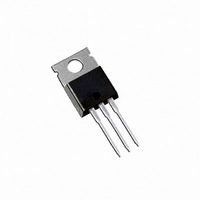
MOSFET N-CH 60V 30A TO-220AB

IRFZ34

Manufacturer Part Number
IRFZ34
Description
MOSFET N-CH 60V 30A TO-220AB
Manufacturer
Vishay
Datasheet

Specifications of IRFZ34

Fet Type
MOSFET N-Channel, Metal Oxide
Fet Feature
Standard
Rds On (max) @ Id, Vgs
50 mOhm @ 18A, 10V
Drain To Source Voltage (vdss)
60V
Current - Continuous Drain (id) @ 25° C
30A
Vgs(th) (max) @ Id
4V @ 250µA
Gate Charge (qg) @ Vgs
46nC @ 10V
Input Capacitance (ciss) @ Vds
1200pF @ 25V
Power - Max
88W
Mounting Type
Through Hole
Package / Case
TO-220-3 (Straight Leads)
Lead Free Status / RoHS Status
Contains lead / RoHS non-compliant
Other names
*IRFZ34

Available stocks

Company
Part Number
Manufacturer
Quantity
Price
Part Number:
IRFZ34
Manufacturer:
IR
Quantity:
1 550
Part Number:
IRFZ34
Manufacturer:
IR
Quantity:
5 510
Part Number:
IRFZ34
Manufacturer:
TOSHIBA
Quantity:
5 510
Part Number:
IRFZ34/N
Manufacturer:
IR
Quantity:
12 500
Part Number:
IRFZ34A
Manufacturer:
FAIRCHILD
Quantity:
1 492
Company:
Part Number:
IRFZ34E
Quantity:
70 000
Company:
Part Number:
IRFZ34L
Quantity:
50 000
Part Number:
IRFZ34N
Manufacturer:
IR墨西哥产地
Quantity:
20 000
Part Number:
IRFZ34NPBF
Manufacturer:
ST
0
Part Number:
IRFZ34NPBF
Manufacturer:
IR
Quantity:
20 000
Company:
Part Number:
IRFZ34NPBF
Quantity:
20 000
Company:
Part Number:
IRFZ34NPBF
Quantity:
30 000
Note
a. See device orientation.
Notes
a. Repetitive rating; pulse width limited by maximum junction temperature (see fig. 11).
b. V
c. I
d. 1.6 mm from case.
e. Uses IRFZ34, SiHFZ34 data and test conditions.
* Pb containing terminations are not RoHS compliant, exemptions may apply
Document Number: 90368
S10-2476-Rev. B, 01-Nov-10
I
2
PRODUCT SUMMARY
V
R
Q
Q
Q
Configuration
ORDERING INFORMATION
Package
Lead (Pb)-free and Halogen-free
Lead (Pb)-free
SnPb
ABSOLUTE MAXIMUM RATINGS (T
PARAMETER
Drain-Source Voltage
Gate-Source Voltage
Continuous Drain Current
Pulsed Drain Current
Linear Derating Factor
Single Pulse Avalanche Energy
Maximum Power Dissipation
Peak Diode Recovery dV/dt
Operating Junction and Storage Temperature Range
Soldering Recommendations (Peak Temperature)
PAK
DS
DS(on)
g
gs
gd
SD
DD
(Max.) (nC)
(nC)
(V)
(nC)
 30 A, dI/dt  200 A/μs, V
= 25 V, Starting T
(TO-262)
()
G
D
S
G
a, e
D
D
J
2
PAK (TO-263)
= 25 °C, L = 260 μH, R
S
c, e
b, e
DD
V
GS
 V
= 10 V
DS
D
-
IRFZ34SPbF
SiHFZ34S-E3
IRFZ34S
SiHFZ34S
, T
2
PAK (TO-263)
G
J
Single
 175 °C.
N-Channel MOSFET
60
46
11
22
g
= 25 , I
C
= 25 °C, unless otherwise noted)
Power MOSFET
D
S
0.050
V
IRFZ34S, IRFZ34L, SiHFZ34S, SiHFZ34L
GS
AS
at 10 V
= 30 A (see fig. 12).
T
T
for 10 s
C
A
D
-
IRFZ34STRRPbF
SiHFZ34STRPbF
IRFZ34STRR
SiHFZ34STR
= 25 °C
= 25 °C
2
PAK (TO-263)
T
T
C
C
= 100 °C
= 25 °C
FEATURES
• Halogen-free According to IEC 61249-2-21
• Advanced Process Technology
• Surface Mount
• Low-Profile Through-Hole (IRFZ34L, SiHFZ34L)
• 175 °C Operating Temperature
• Fast Switching
• Compliant to RoHS Directive 2002/95/EC
DESCRIPTION
Third generation Power MOSFETs from Vishay utilize
advanced processing techniques to achieve extremely low
on-resistance per silicon area. This benefit, combined with
the fast switching speed and ruggedized device design that
Power MOSFETs are well known for, provides the designer
with an extremely efficient and reliable device for use in a
wide variety of applications.
The D
accommodating die sizes up to HEX-4. It provides the
highest
on-resistance in any existing surface mount package. The
D
its low internal connection resistance and can dissipate up
to 2 W in a typical surface mount application.
The through-hole version (IRFZ34L, SiHFZ34L) is available
for low-profile applications.
2
Definition
PAK is suitable for high current applications because of
a
a
2
PAKis a surface mount power package capable of
a
a
power
SYMBOL
T
dV/dt
J
V
V
E
I
, T
P
DM
I
GS
DS
AS
D
D
D
SiHFZ34STRL-GE3
IRFZ34STRLPbF
SiHFZ34STLPbF
IRFZ34STRL
SiHFZ34STL
stg
2
PAK (TO-263)
capability
a
a
- 55 to + 175
a
a
and
LIMIT
300
± 20
0.59
120
200
3.7
4.5
60
30
21
88
Vishay Siliconix
d
the
I
-
IRFZ34LPbF
SiHFZ34L-E3
IRFZ34L
SiHFZ34L
2
PAK (TO-262)
lowest
www.vishay.com
UNIT
W/°C
V/ns
possible
mJ
°C
W
V
A
1

Related parts for IRFZ34

IRFZ34 Summary of contents

Page 1

... A, dI/dt  200 A/μs, V  1.6 mm from case. e. Uses IRFZ34, SiHFZ34 data and test conditions containing terminations are not RoHS compliant, exemptions may apply Document Number: 90368 S10-2476-Rev. B, 01-Nov-10 IRFZ34S, IRFZ34L, SiHFZ34S, SiHFZ34L Power MOSFET FEATURES • Halogen-free According to IEC 61249-2-21 ...

Page 2

... Body Diode Reverse Recovery Time Body Diode Reverse Recovery Charge Forward Turn-On Time Notes a. Repetitive rating; pulse width limited by maximum junction temperature (see fig. 11). b. Pulse width  300 μs; duty cycle  Uses IRFZ34, SiHFZ34 data and test conditions. www.vishay.com 2 SYMBOL TYP. R ...

Page 3

... TYPICAL CHARACTERISTICS (25 °C, unless otherwise noted) Fig Typical Output Characteristics Fig Typical Output Characteristics Document Number: 90368 S10-2476-Rev. B, 01-Nov-10 IRFZ34S, IRFZ34L, SiHFZ34S, SiHFZ34L Fig Typical Transfer Characteristics Fig Normalized On-Resistance vs. Temperature Vishay Siliconix www.vishay.com 3 ...

Page 4

... IRFZ34S, IRFZ34L, SiHFZ34S, SiHFZ34L Vishay Siliconix Fig Typical Capacitance vs. Drain-to-Source Voltage Fig Typical Gate Charge vs. Gate-to-Source Voltage www.vishay.com 4 Fig Typical Source-Drain Diode Forward Voltage Fig Maximum Safe Operating Area Document Number: 90368 S10-2476-Rev. B, 01-Nov-10 ...

Page 5

... Fig Maximum Drain Current vs. Case Temperature Fig Maximum Effective Transient Thermal Impedance, Junction-to-Case Document Number: 90368 S10-2476-Rev. B, 01-Nov-10 IRFZ34S, IRFZ34L, SiHFZ34S, SiHFZ34L Pulse width ≤ 1 µs Duty factor ≤ 0.1 % Fig. 10a - Switching Time Test Circuit d(on) Fig. 10b - Switching Time Waveforms ...

Page 6

... IRFZ34S, IRFZ34L, SiHFZ34S, SiHFZ34L Vishay Siliconix Vary t to obtain p required D.U. 0. Fig. 12a - Unclamped Inductive Test Circuit Fig. 12c - Maximum Avalanche Energy vs. Drain Current Charge Fig. 13a - Maximum Avalanche Energy vs. Drain Current www.vishay.com Fig. 12b - Unclamped Inductive Waveforms Current regulator Same type as D.U.T. ...

Page 7

... Technology and Package Reliability represent a composite of all qualified locations. For related documents such as package/tape drawings, part marking, and reliability data, see www.vishay.com/ppg?90368. Document Number: 90368 S10-2476-Rev. B, 01-Nov-10 IRFZ34S, IRFZ34L, SiHFZ34S, SiHFZ34L Peak Diode Recovery dV/dt Test Circuit + Circuit layout considerations • Low stray inductance • ...

Page 8

... Vishay product could result in personal injury or death. Customers using or selling Vishay products not expressly indicated for use in such applications their own risk and agree to fully indemnify and hold Vishay and its distributors harmless from and against any and all claims, liabilities, expenses and damages arising or resulting in connection with such use or sale, including attorneys fees, even if such claim alleges that Vishay or its distributor was negligent regarding the design or manufacture of the part ...

Related keywords