IRFL024ZPBF International Rectifier, IRFL024ZPBF Datasheet - Page 2
IRFL024ZPBF
Manufacturer Part Number
IRFL024ZPBF
Description
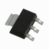
MOSFET N-CH 55V 5.1A SOT223
Manufacturer
International Rectifier
Series
HEXFET®r
Specifications of IRFL024ZPBF
Fet Type
MOSFET N-Channel, Metal Oxide
Fet Feature
Logic Level Gate
Rds On (max) @ Id, Vgs
57.5 mOhm @ 3.1A, 10V
Drain To Source Voltage (vdss)
55V
Current - Continuous Drain (id) @ 25° C
5.1A
Vgs(th) (max) @ Id
4V @ 250µA
Gate Charge (qg) @ Vgs
14nC @ 10V
Input Capacitance (ciss) @ Vds
340pF @ 25V
Power - Max
1W
Mounting Type
Surface Mount
Package / Case
SOT-223 (3 leads + Tab), SC-73, TO-261
Current, Drain
5.1 A
Gate Charge, Total
9.1 nC
Package Type
SOT-223
Polarization
N-Channel
Power Dissipation
1 W
Resistance, Drain To Source On
46.2 Milliohms
Temperature, Operating, Maximum
+150 °C
Temperature, Operating, Minimum
-55 °C
Time, Turn-off Delay
30 ns
Time, Turn-on Delay
7.8 ns
Transconductance, Forward
6.2 S
Voltage, Breakdown, Drain To Source
55 V
Voltage, Forward, Diode
1.3 V
Voltage, Gate To Source
±20 V
Configuration
Single Dual Drain
Transistor Polarity
N-Channel
Resistance Drain-source Rds (on)
57.5 m Ohms
Drain-source Breakdown Voltage
55 V
Gate-source Breakdown Voltage
20 V
Continuous Drain Current
5.1 A
Maximum Operating Temperature
+ 150 C
Mounting Style
SMD/SMT
Fall Time
23 ns
Gate Charge Qg
9.1 nC
Minimum Operating Temperature
- 55 C
Rise Time
21 ns
Lead Free Status / RoHS Status
Lead free / RoHS Compliant
Other names
*IRFL024ZPBF


Notes:
‚
ƒ
„
V
R
V
gfs
I
I
Q
Q
Q
t
t
t
t
C
C
C
C
C
C
I
I
V
t
Q
t
Electrical Characteristics @ T
Source-Drain Ratings and Characteristics
DSS
GSS
d(on)
r
d(off)
f
S
SM
rr
on
V
(BR)DSS
GS(th)
SD
2
DS(on)
iss
oss
rss
oss
oss
oss
g
gs
gd
rr
Part not recommended for use above this value.
V
charging time as C
Repetitive rating; pulse width limited by
R
Pulse width
C
(BR)DSS
max. junction temperature. (See fig. 11).
Limited by T
DSS
G
oss
eff.
= 25 , I
.
eff. is a fixed capacitance that gives the same
/ T
J
AS
Jmax
Drain-to-Source Breakdown Voltage
Breakdown Voltage Temp. Coefficient
Static Drain-to-Source On-Resistance
Gate Threshold Voltage
Forward Transconductance
Drain-to-Source Leakage Current
Gate-to-Source Forward Leakage
Gate-to-Source Reverse Leakage
Total Gate Charge
Gate-to-Source Charge
Gate-to-Drain ("Miller") Charge
Turn-On Delay Time
Rise Time
Turn-Off Delay Time
Fall Time
Input Capacitance
Output Capacitance
Reverse Transfer Capacitance
Output Capacitance
Output Capacitance
Effective Output Capacitance
Continuous Source Current
(Body Diode)
Pulsed Source Current
(Body Diode)
Diode Forward Voltage
Reverse Recovery Time
Reverse Recovery Charge
Forward Turn-On Time
= 3.1A, V
1.0ms; duty cycle
, starting T
oss
Parameter
while V
GS
=10V.
Parameter
J
™
= 25°C, L = 2.8mH
DS
is rising from 0 to 80%
2%.
J
= 25°C (unless otherwise specified)
Intrinsic turn-on time is negligible (turn-on is dominated by LS+LD)
Min. Typ. Max. Units
Min. Typ. Max. Units
–––
–––
–––
–––
–––
–––
–––
–––
–––
–––
–––
–––
–––
–––
–––
–––
–––
–––
–––
–––
–––
–––
–––
–––
2.0
6.2
55
0.053
46.2
–––
–––
–––
–––
–––
–––
–––
340
210
–––
–––
–––
9.1
1.9
3.9
7.8
9.8
…
†
‡
ˆ
21
30
23
68
39
55
93
15
Limited by T
This value determined from sample failure population.
100% tested to this value in production.
When mounted on 1 inch square copper board.
When mounted on FR-4 board using minimum
recommended footprint.
repetitive avalanche performance.
57.5
-200
–––
250
200
–––
–––
–––
–––
–––
–––
–––
–––
–––
–––
–––
–––
–––
–––
4.0
5.1
1.3
20
14
41
23
15
V/°C
m
Jmax
µA
nA
nC
nC
ns
pF
ns
V
V
A
V
S
, see Fig.12a, 12b, 15, 16 for typical
V
Reference to 25°C, I
V
V
V
V
V
V
V
I
V
V
V
I
R
V
V
V
ƒ = 1.0MHz
V
V
V
MOSFET symbol
showing the
integral reverse
p-n junction diode.
T
T
di/dt = 100A/µs
D
D
J
J
GS
GS
DS
DS
DS
DS
GS
GS
DS
GS
DD
GS
GS
DS
GS
GS
GS
G
= 3.1A
= 3.1A
= 25°C, I
= 25°C, I
= 53
= 0V, I
= 10V, I
= V
= 25V, I
= 55V, V
= 55V, V
= 20V
= -20V
= 44V
= 10V
= 28V
= 10V
= 0V
= 25V
= 0V, V
= 0V, V
= 0V, V
GS
, I
D
e
e
Conditions
Conditions
D
DS
S
F
D
D
DS
DS
= 250µA
GS
GS
= 250µA
= 3.1A, V
= 3.1A
= 3.1A, V
= 3.1A
= 0V to 44V
= 1.0V, ƒ = 1.0MHz
= 44V, ƒ = 1.0MHz
e
= 0V
= 0V, T
www.irf.com
D
e
= 1mA
DD
J
GS
G
= 125°C
= 28V
= 0V
f
e
S
D
Related parts for IRFL024ZPBF
Image
Part Number
Description
Manufacturer
Datasheet
Request
R

Part Number:
Description:
Power MOSFET(Vdss=55V, Rds(on)=0.075ohm, Id=2.8A)
Manufacturer:
IRF [International Rectifier]
Datasheet:

Part Number:
Description:
SCHOTTKY RECTIFIER
Manufacturer:
International Rectifier Corp.
Datasheet:
Part Number:
Description:
SCHOTTKY RECTIFIER
Manufacturer:
International Rectifier Corp.
Datasheet:
Part Number:
Description:
SCHOTTKY RECTIFIER
Manufacturer:
International Rectifier Corp.
Datasheet:
Part Number:
Description:
SCHOTTKY RECTIFIER
Manufacturer:
International Rectifier Corp.
Datasheet:
Part Number:
Description:
SCHOTTKY RECTIFIER
Manufacturer:
International Rectifier Corp.
Datasheet:
Part Number:
Description:
SCHOTTKY RECTIFIER
Manufacturer:
International Rectifier Corp.
Datasheet:
Part Number:
Description:
SCHOTTKY RECTIFIER
Manufacturer:
International Rectifier Corp.
Datasheet:
Part Number:
Description:
SCHOTTKY RECTIFIER
Manufacturer:
International Rectifier Corp.
Datasheet:
Part Number:
Description:
SCHOTTKY RECTIFIER
Manufacturer:
International Rectifier Corp.
Datasheet:
Part Number:
Description:
SCHOTTKY RECTIFIER
Manufacturer:
International Rectifier Corp.
Datasheet:
Part Number:
Description:
SCHOTTKY RECTIFIER
Manufacturer:
International Rectifier Corp.
Datasheet:
Part Number:
Description:
SCHOTTKY RECTIFIER
Manufacturer:
International Rectifier Corp.
Datasheet:
Part Number:
Description:
SCHOTTKY RECTIFIER
Manufacturer:
International Rectifier Corp.
Datasheet:
Part Number:
Description:
SCHOTTKY RECTIFIER
Manufacturer:
International Rectifier Corp.
Datasheet: