IRF9540NSPBF International Rectifier, IRF9540NSPBF Datasheet
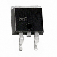
MOSFET P-CH 100V 23A D2PAK

IRF9540NSPBF

Manufacturer Part Number
IRF9540NSPBF
Description
MOSFET P-CH 100V 23A D2PAK
Manufacturer
International Rectifier
Series
HEXFET®r
Type
Power MOSFETr
Datasheets

Specifications of IRF9540NSPBF

Fet Type
MOSFET P-Channel, Metal Oxide
Fet Feature
Standard
Rds On (max) @ Id, Vgs
117 mOhm @ 14A, 10V
Drain To Source Voltage (vdss)
100V
Current - Continuous Drain (id) @ 25° C
23A
Vgs(th) (max) @ Id
4V @ 250µA
Gate Charge (qg) @ Vgs
110nC @ 10V
Input Capacitance (ciss) @ Vds
1450pF @ 25V
Power - Max
3.1W
Mounting Type
Surface Mount
Package / Case
D²Pak, TO-263 (2 leads + tab)
Channel Type
P
Current, Drain
-23 A
Gate Charge, Total
97 nC
Package Type
D2Pak
Polarization
P-Channel
Power Dissipation
140 W
Resistance, Drain To Source On
0.117 Ohm
Temperature, Operating, Maximum
+175 °C
Temperature, Operating, Minimum
-55 °C
Time, Turn-off Delay
51 ns
Time, Turn-on Delay
15 ns
Transconductance, Forward
5.3 S
Voltage, Breakdown, Drain To Source
-100 V
Voltage, Drain To Source
–100 V
Voltage, Forward, Diode
-1.6 V
Voltage, Gate To Source
±20 V
Number Of Elements
1
Polarity
P
Channel Mode
Enhancement
Drain-source On-res
0.117Ohm
Drain-source On-volt
100V
Gate-source Voltage (max)
±20V
Continuous Drain Current
23A
Output Power (max)
Not RequiredW
Frequency (max)
Not RequiredMHz
Noise Figure
Not RequireddB
Power Gain
Not RequireddB
Drain Efficiency
Not Required%
Operating Temp Range
-55C to 175C
Operating Temperature Classification
Military
Mounting
Surface Mount
Pin Count
2 +Tab
Configuration
Single
Transistor Polarity
P-Channel
Resistance Drain-source Rds (on)
117 m Ohms
Drain-source Breakdown Voltage
- 100 V
Gate-source Breakdown Voltage
20 V
Maximum Operating Temperature
+ 175 C
Mounting Style
SMD/SMT
Fall Time
51 ns
Gate Charge Qg
64.7 nC
Minimum Operating Temperature
- 55 C
Rise Time
67 ns
Lead Free Status / RoHS Status
Lead free / RoHS Compliant

Available stocks

Company
Part Number
Manufacturer
Quantity
Price
Part Number:
IRF9540NSPBF
Manufacturer:
IR
Quantity:
34 000
Part Number:
IRF9540NSPBF
Manufacturer:
IR
Quantity:
20 000
l
l
l
l
l
l
l
l
www.irf.com
Features of this design are a 150°C junction
operating temperature, fast switching speed and
improved repetitive avalanche rating . These fea-
tures combine to make this design an extremely
efficient and reliable device for use in a wide
variety of other applications.
Absolute Maximum Ratings
I
I
I
P
P
V
E
I
E
dv/dt
T
T
Thermal Resistance
R
R
D
D
DM
AR
J
STG
D
D
GS
AS
AR
θJC
θJA
@ T
@ T
Advanced Process Technology
Ultra Low On-Resistance
150°C Operating Temperature
Fast Switching
Repetitive Avalanche Allowed up to Tjmax
Some Parameters are Different from
IRF9540NS/L
P-Channel
Lead-Free
@T
@T
C
C
A
C
= 25°C
= 100°C
= 25°C
= 25°C
Continuous Drain Current, V
Continuous Drain Current, VGS @ -10V
Pulsed Drain Current
Maximum Power Dissipation
Linear Derating Factor
Gate-to-Source Voltage
Single Pulse Avalanche Energy
Avalanche Current
Repetitive Avalanche Energy
Peak Diode Recovery dv/dt
Operating Junction and
Storage Temperature Range
Soldering Temperature, for 10 seconds
Junction-to-Case
Junction-to-Ambient (PCB Mount, steady state)
Parameter
Parameter
e
GS
@ -10V
d
G
g
IRF9540NSPbF
Gate
G
D
D
2
Pak
300 (1.6mm from case )
G
Typ.
–––
–––
D
S
D
S
-55 to + 150
Max.
Drain
110
± 20
-23
-14
-92
-14
-13
3.1
0.9
84
11
D
Max.
IRF9540NLPbF
1.1
40
D
TO-262
Source
G
S
Units
Units
W/°C
°C/W
V/ns
D
mJ
mJ
°C
W
A
V
A
S
1

Related parts for IRF9540NSPBF

IRF9540NSPBF Summary of contents

Page 1

... E AR dv/dt Peak Diode Recovery dv/dt T Operating Junction and J T Storage Temperature Range STG Soldering Temperature, for 10 seconds Thermal Resistance R Junction-to-Case θJC Junction-to-Ambient (PCB Mount, steady state) R θJA www.irf.com Pak IRF9540NSPbF G Gate Parameter @ -10V Parameter g D Ω TO-262 IRF9540NLPbF D S Drain Source Max ...

Page 2

Electrical Characteristics @ T Parameter V Drain-to-Source Breakdown Voltage (BR)DSS ∆ΒV /∆T Breakdown Voltage Temp. Coefficient DSS J R Static Drain-to-Source On-Resistance DS(on) V Gate Threshold Voltage GS(th) gfs Forward Transconductance I Drain-to-Source Leakage Current DSS I Gate-to-Source Forward Leakage ...

Page 3

VGS TOP -15V -10V -8.0V -7.0V 100 -6.0V -5.5V -5.0V BOTTOM -4. -4.5V ≤60µs PULSE WIDTH Tj = 25°C 0.1 0 Drain-to-Source Voltage (V) 100 25° ...

Page 4

0V MHZ C iss = SHORTED C rss = oss = iss 1000 C oss C ...

Page 5

Case Temperature (° 0.50 0.20 0.10 0.1 0.05 0.02 0.01 0.01 SINGLE PULSE ( THERMAL RESPONSE ) 0.001 1E-006 1E-005 www.irf.com ≤ ...

Page 6

D.U DRIVER -20V 0.01 Ω (BR)DSS Charge 6 350 V DD 300 A 250 200 150 15V 100 ...

Page 7

D.U.T + ‚ -  Driver Gate Drive D.U.T. I Reverse Recovery Current D.U.T. V Re-Applied Voltage Inductor Curent www.irf.com + • • ƒ • • • • Period D = P.W. Waveform SD Body Diode Forward Current ...

Page 8

T HIS IS AN IRF530S WIT H LOT CODE 8024 AS S EMBLED ON WW 02, 2000 IN THE AS S EMBLY LINE "L" INTERNAT IONAL RECTIFIER F530S LOGO AS S EMBLY LOT CODE PART NUMBER ...

Page 9

TO-262 Package Outline Dimensions are shown in millimeters (inches) TO-262 Part Marking Information EXAMPLE: THIS IS AN IRL3103L LOT CODE 1789 AS S EMBLED ON WW 19, 1997 EMBLY LINE "C" Note: "P" in assembly ...

Page 10

Dimensions are shown in millimeters (inches) TRR FEED DIRECTION 1.85 (.073) 1.65 (.065) TRL FEED DIRECTION 330.00 (14.173) MAX. NOTES : 1. COMFORMS TO EIA-418. 2. CONTROLLING DIMENSION: MILLIMETER. 3. DIMENSION MEASURED @ HUB. 4. INCLUDES FLANGE DISTORTION @ ...

Page 11

Note: For the most current drawings please refer to the IR website at: http://www.irf.com/package/ ...

Related keywords