IRF520NPBF International Rectifier, IRF520NPBF Datasheet
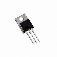
MOSFET N-CH 100V 9.7A TO-220AB

IRF520NPBF

Manufacturer Part Number
IRF520NPBF
Description
MOSFET N-CH 100V 9.7A TO-220AB
Manufacturer
International Rectifier
Series
HEXFET®r
Type
Power MOSFETr
Datasheets

Specifications of IRF520NPBF

Fet Type
MOSFET N-Channel, Metal Oxide
Fet Feature
Standard
Rds On (max) @ Id, Vgs
200 mOhm @ 5.7A, 10V
Drain To Source Voltage (vdss)
100V
Current - Continuous Drain (id) @ 25° C
9.7A
Vgs(th) (max) @ Id
4V @ 250µA
Gate Charge (qg) @ Vgs
25nC @ 10V
Input Capacitance (ciss) @ Vds
330pF @ 25V
Power - Max
48W
Mounting Type
Through Hole
Package / Case
TO-220-3 (Straight Leads)
Current, Drain
9.7 A
Gate Charge, Total
25 nC
Package Type
TO-220AB
Polarization
N-Channel
Power Dissipation
48 W
Resistance, Drain To Source On
0.2 Ohm
Temperature, Operating, Maximum
+175 °C
Temperature, Operating, Minimum
-55 °C
Time, Turn-off Delay
32 ns
Time, Turn-on Delay
4.5 ns
Transconductance, Forward
2.7 S
Voltage, Breakdown, Drain To Source
100 V
Voltage, Forward, Diode
1.3 V
Voltage, Gate To Source
±20 V
Number Of Elements
1
Polarity
N
Channel Mode
Enhancement
Drain-source On-res
0.2Ohm
Drain-source On-volt
100V
Gate-source Voltage (max)
±20V
Continuous Drain Current
9.7A
Output Power (max)
Not RequiredW
Frequency (max)
Not RequiredMHz
Noise Figure
Not RequireddB
Power Gain
Not RequireddB
Drain Efficiency
Not Required%
Operating Temp Range
-55C to 175C
Operating Temperature Classification
Military
Mounting
Through Hole
Pin Count
3 +Tab
Transistor Polarity
N-Channel
Drain-source Breakdown Voltage
100 V
Gate-source Breakdown Voltage
20 V
Mounting Style
Through Hole
Gate Charge Qg
16.7 nC
Lead Free Status / RoHS Status
Lead free / RoHS Compliant
Other names
*IRF520NPBF

Available stocks

Company
Part Number
Manufacturer
Quantity
Price
Part Number:
IRF520NPBF
Manufacturer:
CYPRESS
Quantity:
101
Part Number:
IRF520NPBF
Manufacturer:
IR
Quantity:
20 000
Company:
Part Number:
IRF520NPBF
Quantity:
18 895
Description
Absolute Maximum Ratings
Thermal Resistance
Fifth Generation HEXFETs from International Rectifier
utilize advanced processing techniques to achieve
extremely low on-resistance per silicon area. This
benefit, combined with the fast switching speed and
ruggedized device design that HEXFET Power
MOSFETs are well known for, provides the designer
with an extremely efficient and reliable device for use
in a wide variety of applications.
The TO-220 package is universally preferred for all
commercial-industrial applications at power dissipation
levels to approximately 50 watts. The low thermal
resistance and low package cost of the TO-220
contribute to its wide acceptance throughout the
industry.
I
I
I
P
V
E
I
E
dv/dt
T
T
R
R
R
D
D
DM
AR
J
STG
D
GS
AS
AR
θJC
θCS
θJA
@ T
@ T
Advanced Process Technology
Dynamic dv/dt Rating
175°C Operating Temperature
Fast Switching
Fully Avalanche Rated
Lead-Free
@T
C
C
C
= 25°C
= 100°C
= 25°C
Continuous Drain Current, V
Pulsed Drain Current
Power Dissipation
Linear Derating Factor
Gate-to-Source Voltage
Single Pulse Avalanche Energy
Avalanche Current
Repetitive Avalanche Energy
Peak Diode Recovery dv/dt
Operating Junction and
Storage Temperature Range
Soldering Temperature, for 10 seconds
Mounting torque, 6-32 or M3 srew
Junction-to-Case
Case-to-Sink, Flat, Greased Surface
Junction-to-Ambient
Parameter
Parameter
GS
GS
@ 10V
@ 10V
G
Typ.
300 (1.6mm from case )
0.50
–––
–––
HEXFET
10 lbf•in (1.1N•m)
IRF520NPbF
-55 to + 175
S
D
Max.
TO-220AB
0.32
± 20
9.7
6.8
5.7
4.8
5.0
38
48
91
®
R
Power MOSFET
V
DS(on)
Max.
–––
3.1
DSS
62
I
D
= 9.7A
= 100V
= 0.20Ω
PD - 94818
Units
Units
W/°C
°C/W
V/ns
mJ
mJ
°C
W
A
V
A
11/5/03

Related parts for IRF520NPBF

IRF520NPBF Summary of contents

Page 1

... T Storage Temperature Range STG Soldering Temperature, for 10 seconds Mounting torque, 6- srew Thermal Resistance Parameter R Junction-to-Case θJC R Case-to-Sink, Flat, Greased Surface θCS R Junction-to-Ambient θJA IRF520NPbF HEXFET TO-220AB Max. @ 10V GS @ 10V GS 0.32 - 175 300 (1.6mm from case ) 10 lbf•in (1.1N•m) Typ. ––– ...

Page 2

... IRF520NPbF Electrical Characteristics @ T Parameter V Drain-to-Source Breakdown Voltage (BR)DSS Breakdown Voltage Temp. Coefficient ∆V /∆T (BR)DSS J R Static Drain-to-Source On-Resistance DS(on) V Gate Threshold Voltage GS(th) g Forward Transconductance fs I Drain-to-Source Leakage Current DSS Gate-to-Source Forward Leakage I GSS Gate-to-Source Reverse Leakage Q Total Gate Charge ...

Page 3

... BOTTOM 4. 0.1 100 V , Drain-to-Source Voltage (V) DS Fig 2. Typical Output Characteristics 3 9.5A D 2.5 2.0 1.5 1.0 0.5 0 -60 -40 - Junction Temperature (°C) J Fig 4. Normalized On-Resistance Vs. Temperature IRF520NPbF 4.5V 20µs PULSE WIDTH T = 175° 100 V = 10V 100 120 140 160 180 ...

Page 4

... IRF520NPbF 600 1MHz iss rss gd 500 oss iss 400 C 300 oss 200 C rss 100 Drain-to-Source Voltage (V) DS Fig 5. Typical Capacitance Vs. Drain-to-Source Voltage 100 T = 175° 25° 0.4 0.6 0.8 1 Source-to-Drain Voltage (V) SD Fig 7. Typical Source-Drain Diode Forward Voltage SHORTED ds 16 ...

Page 5

... Fig 11. Maximum Effective Transient Thermal Impedance, Junction-to-Case 10V Pulse Width ≤ 1 µs Duty Factor ≤ 0.1 % Fig 10a. Switching Time Test Circuit V DS 90% 10% 150 175 ° d(on) Fig 10b. Switching Time Waveforms Notes: 1. Duty factor Peak 0.001 t , Rectangular Pulse Duration (sec) 1 IRF520NPbF D.U. d(off ...

Page 6

... IRF520NPbF D.U. 0.01Ω Fig 12a. Unclamped Inductive Test Circuit Fig 12b. Unclamped Inductive Waveforms Charge Fig 13a. Basic Gate Charge Waveform 200 + 160 120 80 V (BR)DSS Starting T , Junction Temperature (°C) Fig 12c. Maximum Avalanche Energy Fig 13b. Gate Charge Test Circuit ...

Page 7

... Waveform DS Diode Recovery Re-Applied Voltage Body Diode Inductor Curent Ripple ≤ for Logic Level Devices GS Fig 14. For N-Channel HEXFETS IRF520NPbF Circuit Layout Considerations • Low Stray Inductance • Ground Plane • Low Leakage Inductance Current Transformer - + + controlled by Duty Factor "D" P.W. ...

Page 8

... IRF520NPbF TO-220AB Package Outline Dimensions are shown in millimeters (inches) 10.54 (.415) 10.29 (.405) 2.87 (.113) 2.62 (.103) 15.24 (.600) 14.84 (.584) 1 14.09 (.555) 13.47 (.530) 1.40 (.055) 3X 1.15 (.045) 2.54 (.100) 2X NOTES: 1 DIMENSIONING & TOLERANCING PER ANSI Y14.5M, 1982. 2 CONTROLLING DIMENSION : INCH ...

Page 9

Note: For the most current drawings please refer to the IR website at: http://www.irf.com/package/ ...

Related keywords