IRF3710ZSTRLPBF International Rectifier, IRF3710ZSTRLPBF Datasheet

MOSFET N-CH 100V 59A D2PAK

IRF3710ZSTRLPBF

Manufacturer Part Number
IRF3710ZSTRLPBF
Description
MOSFET N-CH 100V 59A D2PAK
Manufacturer
International Rectifier
Series
HEXFET®r
Datasheet

Specifications of IRF3710ZSTRLPBF

Package / Case
D²Pak, TO-263 (2 leads + tab)
Mounting Type
Surface Mount
Power - Max
160W
Fet Type
MOSFET N-Channel, Metal Oxide
Gate Charge (qg) @ Vgs
120nC @ 10V
Vgs(th) (max) @ Id
4V @ 250µA
Current - Continuous Drain (id) @ 25° C
59A
Drain To Source Voltage (vdss)
100V
Fet Feature
Standard
Rds On (max) @ Id, Vgs
18 mOhm @ 35A, 10V
Transistor Polarity
N Channel
Continuous Drain Current Id
59A
Drain Source Voltage Vds
100V
On Resistance Rds(on)
18mohm
Rds(on) Test Voltage Vgs
10V
Peak Reflow Compatible (260 C)
Yes
Rohs Compliant
Yes
Drain-source Breakdown Voltage
100 V
Gate-source Breakdown Voltage
20 V
Continuous Drain Current
59 A
Power Dissipation
160 W
Mounting Style
SMD/SMT
Gate Charge Qg
82 nC
Lead Free Status / RoHS Status
Lead free / RoHS Compliant
Features
Description
Specifically designed for Automotive applications,
this HEXFET
processing techniques to achieve extremely low
on-resistance per silicon area. Additional fea-
tures of this design are a 175°C junction operating
temperature, fast switching speed and improved
repetitive avalanche rating . These features com-
bine to make this design an extremely efficient
and reliable device for use in Automotive applica-
tions and a wide variety of other applications.
HEXFET
I
I
I
P
V
E
E
I
E
T
T
R
R
R
R
Absolute Maximum Ratings
Thermal Resistance
www.irf.com
D
D
DM
AR
J
STG
D
GS
AS
AS
AR
θJC
θCS
θJA
θJA
@ T
@ T
@T
Advanced Process Technology
Ultra Low On-Resistance
Dynamic dv/dt Rating
175°C Operating Temperature
Fast Switching
Repetitive Avalanche Allowed up to Tjmax
(tested)
C
C
C
= 25°C
= 100°C
= 25°C
®
is a registered trademark of International Rectifier.
®
Power MOSFET utilizes the latest
Continuous Drain Current, V
Pulsed Drain Current
Maximum Power Dissipation
Linear Derating Factor
Gate-to-Source Voltage
Single Pulse Avalanche Energy (Thermally Limited)
Single Pulse Avalanche Energy Tested Value
Avalanche Current
Repetitive Avalanche Energy
Operating Junction and
Storage Temperature Range
Soldering Temperature, for 10 seconds
Mounting torque, 6-32 or M3 screw
Junction-to-Case
Case-to-Sink, Flat, Greased Surface
Junction-to-Ambient
Junction-to-Ambient (PCB Mount, steady state)
c
Parameter
c
Parameter
AUTOMOTIVE MOSFET
GS
GS
h
@ 10V (Silicon Limited)
@ 10V (See Fig. 9)
G
TO-220AB
i
IRF3710Z
j
d
300 (1.6mm from case )
See Fig.12a,12b,15,16
HEXFET
Typ.
0.50
–––
–––
–––
10 lbf•in (1.1N•m)
S
D
-55 to + 175
IRF3710ZS
Max.
D
240
160
± 20
170
200
1.1
59
42
2
Pak
®
IRF3710ZS
R
IRF3710ZL
Power MOSFET
Max.
V
DS(on)
0.92
–––
IRF3710Z
62
40
DSS
I
D
= 59A
PD - 94632A
= 100V
IRF3710ZL
= 18mΩ
TO-262
Units
Units
W/°C
°C/W
mJ
mJ
°C
W
A
V
A
1

Related parts for IRF3710ZSTRLPBF

IRF3710ZSTRLPBF Summary of contents

Page 1

... Soldering Temperature, for 10 seconds Mounting torque, 6- screw Thermal Resistance R Junction-to-Case θJC Case-to-Sink, Flat, Greased Surface R θCS R Junction-to-Ambient θJA R Junction-to-Ambient (PCB Mount, steady state) θJA ® HEXFET is a registered trademark of International Rectifier. www.irf.com AUTOMOTIVE MOSFET G TO-220AB IRF3710Z Parameter @ 10V (Silicon Limited 10V (See Fig Parameter ...

Page 2

Static @ T = 25°C (unless otherwise specified) J Parameter V Drain-to-Source Breakdown Voltage (BR)DSS ∆ΒV /∆T Breakdown Voltage Temp. Coefficient DSS J R Static Drain-to-Source On-Resistance DS(on) V Gate Threshold Voltage GS(th) gfs Forward Transconductance I Drain-to-Source Leakage Current ...

Page 3

VGS TOP 15V 10V 8.0V 100 7.0V 6.0V 5.5V 5.0V 10 BOTTOM 4.5V 1 4.5V 0.1 20µs PULSE WIDTH Tj = 25°C 0.01 0 Drain-to-Source Voltage (V) Fig 1. Typical Output Characteristics 1000 100 10 ...

Page 4

0V MHZ iss rss = 10000 oss ds gd Ciss 1000 Coss 100 ...

Page 5

Case Temperature (°C) Fig 9. Maximum Drain Current vs. Case Temperature 0.50 0.20 0.10 0.1 0.05 0.02 0.01 0.01 SINGLE PULSE ( ...

Page 6

D.U 20V GS 0.01 Ω Fig 12a. Unclamped Inductive Test Circuit V (BR)DSS Fig 12b. Unclamped Inductive Waveforms ...

Page 7

Duty Cycle = Single Pulse 100 0.01 10 0.05 0.10 1 0.1 1.0E-08 1.0E-07 Fig 15. Typical Avalanche Current vs.Pulsewidth 200 TOP Single Pulse BOTTOM 10% Duty Cycle 35A 150 100 ...

Page 8

SD • Fig 17. Fig 18a. Switching Time Test Circuit V DS 90% 10 Fig 18b. Switching Time Waveforms 8 Driver Gate Drive P.W. D.U.T. ...

Page 9

Dimensions are shown in millimeters (inches) 10.54 (.415) 10.29 (.405) 2.87 (.113) 2.62 (.103) 4 15.24 (.600) 14.84 (.584 14.09 (.555) 13.47 (.530) 1.40 (.055) 3X 1.15 (.045) 2.54 (.100) 2X NOTES: 1 DIMENSIONING & TOLERANCING PER ...

Page 10

Dimensions are shown in millimeters (inches HIS IS AN IRF530S WIT H LOT CODE 8024 ASS EMBLED ON WW 02, 2000 ASS EMBLY LINE "L" 10 INT ERNAT IONAL RECT IFIER F530S LOGO AS ...

Page 11

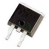
TO-262 Package Outline Dimensions are shown in millimeters (inches) TO-262 Part Marking Information www.irf.com IGBT 1- GATE 2- COLLECTOR 3- EMITTER 11 ...

Page 12

Dimensions are shown in millimeters (inches) TRR FEED DIRECTION 1.85 (.073) 1.65 (.065) TRL 10.90 (.429) 10.70 (.421) FEED DIRECTION 330.00 (14.173) MAX. NOTES : 1. COMFORMS TO EIA-418. 2. CONTROLLING DIMENSION: MILLIMETER. 3. DIMENSION MEASURED @ HUB. 4. ...

Page 13

Note: For the most current drawings please refer to the IR website at: http://www.irf.com/package/ ...

Related keywords