NTD4860NT4G ON Semiconductor, NTD4860NT4G Datasheet

MOSFET N-CH 25V 10.4A DPAK

NTD4860NT4G

Manufacturer Part Number
NTD4860NT4G
Description
MOSFET N-CH 25V 10.4A DPAK
Manufacturer
ON Semiconductor
Datasheet

Specifications of NTD4860NT4G

Fet Type
MOSFET N-Channel, Metal Oxide
Fet Feature
Logic Level Gate
Rds On (max) @ Id, Vgs
7.5 mOhm @ 30A, 10V
Drain To Source Voltage (vdss)
25V
Current - Continuous Drain (id) @ 25° C
10.4A
Vgs(th) (max) @ Id
2.5V @ 250µA
Gate Charge (qg) @ Vgs
16.5nC @ 4.5V
Input Capacitance (ciss) @ Vds
1308pF @ 12V
Power - Max
1.28W
Mounting Type
Surface Mount
Package / Case
DPak, TO-252 (2 leads+tab), SC-63
Configuration
Single
Transistor Polarity
N-Channel
Resistance Drain-source Rds (on)
0.0075 Ohms
Drain-source Breakdown Voltage
25 V
Gate-source Breakdown Voltage
+/- 20 V
Continuous Drain Current
13 A
Power Dissipation
2 W
Maximum Operating Temperature
+ 175 C
Mounting Style
SMD/SMT
Minimum Operating Temperature
- 55 C
Lead Free Status / RoHS Status
Lead free / RoHS Compliant

Available stocks

Company
Part Number
Manufacturer
Quantity
Price
Part Number:
NTD4860NT4G
Manufacturer:
ON
Quantity:
12 500
NTD4860N
Power MOSFET
25 V, 65 A, Single N- -Channel, DPAK/IPAK
Features
Applications
Stresses exceeding Maximum Ratings may damage the device. Maximum
Ratings are stress ratings only. Functional operation above the Recommended
Operating Conditions is not implied. Extended exposure to stresses above the
Recommended Operating Conditions may affect device reliability.
© Semiconductor Components Industries, LLC, 2010
June, 2010 - - Rev. 1
MAXIMUM RATINGS
Drain--to--Source Voltage
Gate--to--Source Voltage
Continuous Drain
Current R
(Note 1)
Power Dissipation
R
Continuous Drain
Current R
(Note 2)
Power Dissipation
R
Continuous Drain
Current R
(Note 1)
Power Dissipation
R
Pulsed Drain
Current
Current Limited by Package
Operating Junction and Storage
Temperature
Source Current (Body Diode)
Drain to Source dV/dt
Single Pulse Drain--to--Source Avalanche
Energy (T
I
Lead Temperature for Soldering Purposes
(1/8” from case for 10 s)
L
Trench Technology
Low R
Low Capacitance to Minimize Driver Losses
Optimized Gate Charge to Minimize Switching Losses
These are Pb- -Free Devices
VCORE Applications
DC- -DC Converters
High/Low Side Switching
θJA
θJA
θJC
= 13 A
(Note 1)
(Note 2)
(Note 1)
DS(on)
pk
θJA
θJA
θJC
J
, L = 1.0 mH, R
= 25°C, V
to Minimize Conduction Losses
Parameter
DD
t
Steady
p
State
=10ms
= 50 V, V
(T
G
J
= 25 Ω)
= 25°C unless otherwise stated)
GS
T
T
T
T
T
T
T
T
T
T
T
A
A
A
A
A
A
C
C
C
A
A
= 10 V,
= 25°C
= 85°C
= 25°C
= 25°C
= 85°C
= 25°C
= 25°C
= 85°C
= 25°C
= 25°C
= 25°C
I
Symbol
DmaxPkg
V
T
dV/dt
EAS
V
I
P
P
P
T
STG
T
DSS
ID
DM
I
I
I
GS
D
D
S
J
D
D
D
L
,
Value
--55 to
+175
10.4
1.28
84.5
±20
130
260
2.0
8.0
25
13
10
65
50
50
45
42
6
1
Unit
V/ns
mJ
°C
°C
W
W
W
V
V
A
A
A
A
A
A
Gate
See detailed ordering and shipping information in the package
dimensions section on page 6 of this data sheet.
CASE 369AA
1
1 2
(Bent Lead)
V
STYLE 2
Drain
Drain 3
(BR)DSS
25 V
DPAK
4
2
3
Source
ORDERING INFORMATION
G
Y
WW
4860N = Device Code
G
MARKING DIAGRAMS
& PIN ASSIGNMENTS
4
N- -CHANNEL MOSFET
http://onsemi.com
Gate
11.1 mΩ @ 4.5 V
7.5 mΩ @ 10 V
(Straight Lead)
R
CASE 369AC
1
= Year
= Work Week
= Pb--Free Package
DS(ON)
Drain
Drain
3 IPAK
1
4
D
2
2 3
Publication Order Number:
3
4
MAX
Source
S
Gate
(Straight Lead
CASE 369D
1
1
NTD4860N/D
Drain
DPAK)
Drain
2
I
IPAK
D
4
65 A
3
2
MAX
3
Source
4

Related parts for NTD4860NT4G

NTD4860NT4G Summary of contents

Page 1

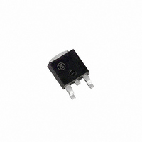
NTD4860N Power MOSFET Single N- -Channel, DPAK/IPAK Features • Trench Technology • Low R to Minimize Conduction Losses DS(on) • Low Capacitance to Minimize Driver Losses • Optimized Gate Charge to Minimize Switching Losses • These ...

Page 2

THERMAL RESISTANCE MAXIMUM RATINGS Parameter Junction--to--Case (Drain) Junction--to--TAB (Drain) Junction--to--Ambient – Steady State (Note 1) Junction--to--Ambient – Steady State (Note 2) 1. Surface--mounted on FR4 board using 1 sq--in pad Cu. 2. Surface--mounted on FR4 board using the ...

Page 3

ELECTRICAL CHARACTERISTICS Parameter DRAIN- -SOURCE DIODE CHARACTERISTICS Forward Diode Voltage Reverse Recovery Time Charge Time Discharge Time Reverse Recovery Charge PACKAGE PARASITIC VALUES Source Inductance Drain Inductance, DPAK Drain Inductance, IPAK Gate Inductance Gate Resistance 3. Pulse Test: pulse width ...

Page 4

V 10V 25° DRAIN--TO--SOURCE VOLTAGE (VOLTS) DS Figure 1. On- -Region Characteristics 0.040 0.036 0.032 0.028 0.024 0.020 0.016 0.012 0.008 0.004 0 ...

Page 5

C iss 1500 1000 C oss 500 C rss DRAIN--TO--SOURCE VOLTAGE (VOLTS) Figure 7. Capacitance Variation 1000 11 100 t ...

Page 6

... SINGLE PULSE 0.01 1.0E--05 1.0E--04 ORDERING INFORMATION Device NTD4860NT4G NTD4860N--1G NTD4860N--35G †For information on tape and reel specifications, including part orientation and tape sizes, please refer to our Tape and Reel Packaging Specifications Brochure, BRD8011/D. TYPICAL PERFORMANCE CURVES P (pk) t ...

Page 7

... DETAIL 0.005 (0.13 *For additional information on our Pb--Free strategy and soldering details, please download the ON Semiconductor Soldering and Mounting Techniques Reference Manual, SOLDERRM/D. PACKAGE DIMENSIONS DPAK (SINGLE GUAGE) CASE 369AA--01 ISSUE GAUGE L2 SEATING C PLANE PLANE DETAIL A ROTATED 90 CW ° SOLDERING FOOTPRINT* 6 ...

Page 8

... Opportunity/Affirmative Action Employer. This literature is subject to all applicable copyright laws and is not for resale in any manner. PUBLICATION ORDERING INFORMATION LITERATURE FULFILLMENT: Literature Distribution Center for ON Semiconductor P.O. Box 5163, Denver, Colorado 80217 USA Phone: 303--675--2175 or 800--344--3860 Toll Free USA/Canada Fax: 303--675--2176 or 800--344--3867 Toll Free USA/Canada Email: orderlit@onsemi ...

Related keywords