IRF530STRL Vishay, IRF530STRL Datasheet
IRF530STRL
Specifications of IRF530STRL
Available stocks


Related parts for IRF530STRL


IRF530STRL Summary of contents
Page 1
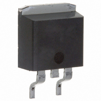
... The PAK (TO-263) is suitable for high current applications because of its low internal connection resistance and can N-Channel MOSFET dissipate typical surface mount application PAK (TO-263) IRF530STRLPbF SiHF530STL-E3 IRF530STRL SiHF530STL = 25 °C, unless otherwise noted ° 100 ° ° ...
Page 2
... IRF530S, SiHF530S Vishay Siliconix THERMAL RESISTANCE RATINGS PARAMETER Maximum Junction-to-Ambient Maximum Junction-to-Ambient a (PCB Mount) Maximum Junction-to-Case (Drain) Note a. When mounted on 1" square PCB (FR-4 or G-10 material). SPECIFICATIONS °C, unless otherwise noted J PARAMETER Static Drain-Source Breakdown Voltage V Temperature Coefficient DS Gate-Source Threshold Voltage ...
Page 3
... Document Number: 91020 S-82996-Rev. A, 19-Jan-09 4 µs Pulse Width ° 91020_03 = 25 ° µs Pulse Width T = 175 ° 91020_04 = 175 °C Fig Normalized On-Resistance vs. Temperature C IRF530S, SiHF530S Vishay Siliconix ° ° 175 µs Pulse Width Gate-to-Source Voltage ( Fig Typical Transfer Characteristics 3.5 ...
Page 4
... IRF530S, SiHF530S Vishay Siliconix 1400 MHz iss gs 1200 rss oss ds 1000 800 600 400 200 Drain-to-Source Voltage ( 91020_05 Fig Typical Capacitance vs. Drain-to-Source Voltage Total Gate Charge (nC) 91020_06 G Fig Typical Gate Charge vs. Gate-to-Source Voltage www.vishay.com Shorted iss C oss C rss 1 91020_07 Fig Typical Source-Drain Diode Forward Voltage ...
Page 5
... Fig Maximum Effective Transient Thermal Impedance, Junction-to-Case Document Number: 91020 S-82996-Rev. A, 19-Jan-09 125 150 175 Single Pulse (Thermal Response Rectangular Pulse Duration (s) 1 IRF530S, SiHF530S Vishay Siliconix D.U. Pulse width ≤ 1 µs Duty factor ≤ 0.1 % Fig. 10a - Switching Time Test Circuit ...
Page 6
... IRF530S, SiHF530S Vishay Siliconix Vary t to obtain p required I AS D.U 0.01 Ω Fig. 12a - Unclamped Inductive Test Circuit 91020_12c Fig. 12c - Maximum Avalanche Energy vs. Drain Current Charge Fig. 13a - Basic Gate Charge Waveform www.vishay.com Fig. 12b - Unclamped Inductive Waveforms 200 Top ...
Page 7
... V GS Vishay Siliconix maintains worldwide manufacturing capability. Products may be manufactured at one of several qualified locations. Reliability data for Silicon Technology and Package Reliability represent a composite of all qualified locations. For related documents such as package/tape drawings, part marking, and reliability data, see www.vishay.com/ppg?91020. Document Number: 91020 S-82996-Rev ...
Page 8
... Vishay disclaims any and all liability arising out of the use or application of any product described herein or of any information provided herein to the maximum extent permitted by law. The product specifications do not expand or otherwise modify Vishay’ ...