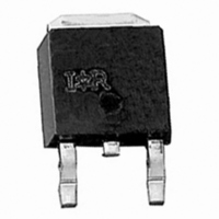
IRLR3715Z International Rectifier, IRLR3715Z Datasheet - Page 8

IRLR3715Z
Manufacturer Part Number
IRLR3715Z
Description
MOSFET N-CH 20V 49A DPAK
Manufacturer
International Rectifier
Series
HEXFET®r
Datasheet
1.IRLR3715ZTRRPBF.pdf
(12 pages)
Specifications of IRLR3715Z
Fet Type
MOSFET N-Channel, Metal Oxide
Fet Feature
Logic Level Gate
Rds On (max) @ Id, Vgs
11 mOhm @ 15A, 10V
Drain To Source Voltage (vdss)
20V
Current - Continuous Drain (id) @ 25° C
49A
Vgs(th) (max) @ Id
2.55V @ 250µA
Gate Charge (qg) @ Vgs
11nC @ 4.5V
Input Capacitance (ciss) @ Vds
810pF @ 10V
Power - Max
40W
Mounting Type
Surface Mount
Package / Case
DPak, TO-252 (2 leads+tab), SC-63
Lead Free Status / RoHS Status
Contains lead / RoHS non-compliant
Other names
*IRLR3715Z
Available stocks
Company
Part Number
Manufacturer
Quantity
Price
Company:
Part Number:
IRLR3715Z
Manufacturer:
IR
Quantity:
12 500
Part Number:
IRLR3715Z
Manufacturer:
IR
Quantity:
20 000
Part Number:
IRLR3715ZC
Manufacturer:
IR
Quantity:
20 000
Company:
Part Number:
IRLR3715ZCPBF
Manufacturer:
INTERNATIONAL RECTIFIER
Quantity:
30 000
Company:
Part Number:
IRLR3715ZCPBF
Manufacturer:
IR
Quantity:
12 500
Company:
Part Number:
IRLR3715ZPBF
Manufacturer:
IR
Quantity:
40 000
Part Number:
IRLR3715ZTRPBF
Manufacturer:
IR
Quantity:
20 000
Control FET
P
P
Power MOSFET Selection for Non-Isolated DC/DC Converters
loss
8
loss
This can be expanded and approximated by;
= I
+ I ×
+ Q
+
= P
(
(
Q
rms
conduction
g
2
oss
× V
2
Q
× R
i
× V
g
gd
g
× f
ds(on )
in
× V
+ P
× f
)
in
)
switching
× f
+ I ×
+ P
drive
Q
+ P
i
gs 2
g
× V
output
in
× f
Synchronous FET
by;
*dissipated primarily in Q1.
portant characteristic; however, once again the im-
portance of gate charge must not be overlooked since
it impacts three critical areas. Under light load the
MOSFET must still be turned on and off by the con-
trol IC so the gate drive losses become much more
significant. Secondly, the output charge Q
verse recovery charge Q
are transfered to Q1 and increase the dissipation in
that device. Thirdly, gate charge will impact the
MOSFETs’ susceptibility to Cdv/dt turn on.
of the converter and therefore sees transitions be-
tween ground and V
a rate of change of drain voltage dV/dt which is ca-
pacitively coupled to the gate of Q2 and can induce
a voltage spike on the gate that is sufficient to turn
the MOSFET on, resulting in shoot-through current .
The ratio of Q
potential for Cdv/dt turn on.
Figure A: Q
P
P
loss
loss
The power loss equation for Q2 is approximated
For the synchronous MOSFET Q2, R
The drain of Q2 is connected to the switching node
= P
= I
+ Q
+
(
(
conduction
rms
Q
oss
g
2
oss
2
× V
Characteristic
gd
× R
/Q
× V
g
gs1
+ P
ds(on)
× f
in
in
must be minimized to reduce the
. As Q1 turns on and off there is
drive
× f
)
)
rr
+ P
both generate losses that
+ Q
output
(
*
rr
× V
www.irf.com
in
ds(on)
× f
oss
is an im-
and re-
)


