IRFR3412PBF International Rectifier, IRFR3412PBF Datasheet
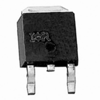
MOSFET N-CH 100V 48A DPAK

IRFR3412PBF

Manufacturer Part Number
IRFR3412PBF
Description
MOSFET N-CH 100V 48A DPAK
Manufacturer
International Rectifier
Series
HEXFET®r
Datasheet

Specifications of IRFR3412PBF

Fet Type
MOSFET N-Channel, Metal Oxide
Fet Feature
Standard
Rds On (max) @ Id, Vgs
25 mOhm @ 29A, 10V
Drain To Source Voltage (vdss)
100V
Current - Continuous Drain (id) @ 25° C
48A
Vgs(th) (max) @ Id
5.5V @ 250µA
Gate Charge (qg) @ Vgs
89nC @ 10V
Input Capacitance (ciss) @ Vds
3430pF @ 25V
Power - Max
140W
Mounting Type
Surface Mount
Package / Case
DPak, TO-252 (2 leads+tab), SC-63
Lead Free Status / RoHS Status
Lead free / RoHS Compliant
Other names
*IRFR3412PBF
l
l
l
l
l
l
l
l
l
Applications
Benefits
Diode Characteristics
www.irf.com
Absolute Maximum Ratings
I
I
I
P
V
dv/dt
T
T
Symbol
I
I
V
t
Q
I
t
D
D
DM
S
SM
rr
RRM
on
J
STG
D
GS
SD
rr
Drive Requirement
dv/dt Ruggedness
Avalanche Voltage and Current
@ T
@ T
Switch Mode Power Supply (SMPS)
Motor Drive
Lead-Free
Low Gate Charge Qg results in Simple
Improved Gate, Avalanche and Dynamic
Fully Characterized Capacitance and
Enhanced Body Diode dv/dt Capability
@T
Bridge Converters
All Zero Voltage Switching
C
C
C
= 25°C
= 100°C
= 25°C
Continuous Source Current
(Body Diode)
Pulsed Source Current
(Body Diode) 
Diode Forward Voltage
Reverse Recovery Time
Reverse RecoveryCharge
Reverse RecoveryCurrent
Forward Turn-On Time
Continuous Drain Current, V
Pulsed Drain Current 
Power Dissipation
Linear Derating Factor
Gate-to-Source Voltage
Peak Diode Recovery dv/dt ƒ
Operating Junction and
Storage Temperature Range
Soldering Temperature, for 10 second
Mounting torqe, 6-32 or M3 screw
Parameter
Parameter
SMPS MOSFET
GS
GS
@ 10V
@ 10V
Min. Typ. Max. Units
–––
–––
–––
–––
–––
–––
Intrinsic turn-on time is negligible (turn-on is dominated by L
–––
–––
–––
160
4.5
68
48
V
100V
100
240
1.3
6.8
190
DSS
300(1.6mm from case )
nC
10 lbf•in (1.1N•m)
ns
V
A
-55 to + 175
IRFR3412
HEXFET Power MOSFET
D-Pak
Max.
MOSFET symbol
showing the
integral reverse
p-n junction diode.
T
T
di/dt = 100A/µs „
48
34
0.95
190
140
± 20
6.4
J
J
R
= 25°C, I
= 125°C, I
DS(on)
0.025Ω
IRFR3412PbF
IRFU3412PbF
S
Conditions
F
= 29A, V
= 29A
IRFU3412
max
I-Pak
GS
= 0V „
G
Units
W/°C
V/ns
°C
W
A
V
48A†
S
+L
12/03/04
I
D
D
D
S
)
1

Related parts for IRFR3412PBF

IRFR3412PBF Summary of contents

Page 1

... T ––– 68 100 ns T di/dt = 100A/µs „ ––– 160 240 nC ––– 4.5 6.8 A Intrinsic turn-on time is negligible (turn-on is dominated by L IRFR3412PbF IRFU3412PbF R max I DS(on) D 0.025Ω 48A† I-Pak IRFU3412 Units † † A 190 140 W 0 ...

Page 2

Static @ T = 25°C (unless otherwise specified) J Parameter V Drain-to-Source Breakdown Voltage (BR)DSS ∆V Breakdown Voltage Temp. Coefficient /∆T (BR)DSS J R Static Drain-to-Source On-Resistance DS(on) V Gate Threshold Voltage GS(th) I Drain-to-Source Leakage Current DSS Gate-to-Source Forward ...

Page 3

VGS TOP 15V 10V 8.0V 7.0V 6.0V 100 5.5V 5.0V BOTTOM 4. 0.1 4.5V 20µs PULSE WIDTH 0.01 0 Drain-to-Source Voltage (V) DS Fig 1. Typical Output Characteristics 1000 100 ...

Page 4

0V MHZ C iss = SHORTED C rss = oss = 10000 Ciss 1000 Coss Crss 100 1 10 ...

Page 5

LIMITED BY PACKAGE 100 T , Case Temperature C Fig 9. Maximum Drain Current Vs. Case Temperature 0.50 0.20 0.10 0.1 0.05 SINGLE PULSE 0.02 (THERMAL RESPONSE) ...

Page 6

D.U 20V GS 0.01 Ω Fig 12a. Unclamped Inductive Test Circuit Fig 12b. Unclamped Inductive Waveforms Charge ...

Page 7

D.U.T + ‚ -  Driver Gate Drive P.W. D.U.T. I Waveform SD Reverse Recovery Current D.U.T. V Waveform DS Re-Applied Voltage Inductor Curent Fig 14. For N-Channel HEXFET www.irf.com + • • ƒ • - „ • ...

Page 8

EXAMPLE: T HIS IS AN IRF R120 WIT EMBLY LOT CODE 1234 ASS EMBLED ON WW 16, 1999 IN THE ASS EMBLY LINE "A" Note: "P" embly line position indicates "Lead-F ree" OR INT ...

Page 9

EXAMPLE: THIS IS AN IRF U120 WITH ASSEMBLY LOT CODE 5678 ASSEMBLED ON WW 19, 1999 IN THE ASSEMBLY LINE "A" Note: "P" embly line pos ition indicates "Lead-Free" OR INT ERNAT IONAL RECTIF IER LOGO www.irf.com ...

Page 10

NOTES : 1. CONTROLLING DIMENSION : MILLIMETER. 2. ALL DIMENSIONS ARE SHOWN IN MILLIMETERS ( INCHES ). 3. OUTLINE CONFORMS TO EIA-481 & EIA-541. 13 INCH NOTES : 1. OUTLINE CONFORMS TO ...

Page 11

Note: For the most current drawings please refer to the IR website at: http://www.irf.com/package/ ...

Related keywords