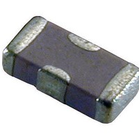
V3F418A400Y3GDP AVX Corporation, V3F418A400Y3GDP Datasheet - Page 7

V3F418A400Y3GDP
Manufacturer Part Number
V3F418A400Y3GDP
Description
Varistors 18 VDC 42v 150pF .1 J
Manufacturer
AVX Corporation
Series
V2Fr
Datasheet
1.V3F418A400Y3GDP.pdf
(8 pages)
Specifications of V3F418A400Y3GDP
Technology
Multilayer Array
Capacitance Value
150pF
Clamping Current
1A
Clamping Voltage
42V
Ac Voltage Rating (max)
13VAC
Dc Voltage Rating (max)
18VDC
Mounting
Surface Mount
Surge Current (max)
20A
Size Code
0612
Lead Spacing
0.76mm
Product Length (mm)
1.6mm
Product Depth (mm)
3.25mm
Product Height (mm)
1.22mm
Energy
0.1Joule
Varistor Voltage
25.5V
Product
MLV
Voltage Rating Dc
18 V
Voltage Rating Ac
13 V
Peak Surge Current
20 A
Surge Energy Rating
0.1 J
Capacitance
150 pF
Dimensions
1.25 mm W x 2.01 mm L x 1.143 mm H
Package / Case
0805 (2012 mm)
Lead Free Status / RoHS Status
Compliant
TransFeed
AVX Multilayer Ceramic Transient Voltage Suppressors
TVS Protection and EMI Attenuation in a Single Chip
PERFORMANCE CHARACTERISTICS
FEEDTHRU VARISTORS
AVX Multilayer Feedthru Varistors (MLVF) are an ideal choice
for system designers with transient strike and broadband
EMI/RFI concerns.
Feedthru Varistors utilize a ZnO varistor material and the
electrode pattern of a feedthru capacitor. This combination
allows the package advantage of the feedthru and material
advantages of the ZnO dielectric to be optimized.
ZnO MLV Feedthrus exhibit electrical and physical advantages
over standard ZnO MLVs. Among them are:
Where: R
1. Faster Turn on Time
2. Broadband EMI attenuation
3. Small size (relative to discrete MLV and EMI filter schemes)
R
C
R
L
p
v
p
on
PCB
Trace
=
≥
=
=
=
Voltage Variable resistance
(per VI curve)
10
defined by voltage rating and energy level
turn on resistance
parallel body inductance
Discrete MLV Model
R
12
V
Ω
Solder Pad
L
R on
C
P
R
P
To Device
Requiring
Protection
The electrical model for a ZnO MLV and a ZnO Feedthru MLV
are shown below. The key difference in the model for
the Feedthru is a transformation in parallel to series induc-
tance. The added series inductance helps lower the injected
transient peak current (by 2πfL) resulting in an additional ben-
efit of a lower clamping voltage. The lowered parallel induc-
tance decreases the turn on time for the varistor to <250ps.
Where: R
Solder Pad
R
C
R
L
L
p
s
v
p
on
=
=
=
=
=
=
R
Discrete MLVF Model
Voltage Variable resistance
(per VI curve)
Body IR
defined by voltage rating and energy level
turn on resistance
minimized parallel body inductance
series body inductance
V
L
S
R on
L
Solder Pad
C
P
L
S
R
P
Solder Pad
To Device
Requiring
Protection
53


