VN2410LZL1G ON Semiconductor, VN2410LZL1G Datasheet
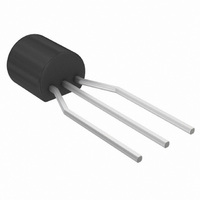
MOSFET N-CH 240V 200MA TO-92

VN2410LZL1G

Manufacturer Part Number
VN2410LZL1G
Description
MOSFET N-CH 240V 200MA TO-92
Manufacturer
ON Semiconductor
Datasheet

Specifications of VN2410LZL1G

Fet Type
MOSFET N-Channel, Metal Oxide
Fet Feature
Standard
Rds On (max) @ Id, Vgs
10 Ohm @ 500mA, 10V
Drain To Source Voltage (vdss)
240V
Current - Continuous Drain (id) @ 25° C
200mA
Vgs(th) (max) @ Id
2V @ 1mA
Input Capacitance (ciss) @ Vds
125pF @ 25V
Power - Max
350mW
Mounting Type
Through Hole
Package / Case
TO-92-3 (Standard Body), TO-226
Lead Free Status / RoHS Status
Lead free / RoHS Compliant
Gate Charge (qg) @ Vgs
-
Other names
VN2410LZL1G
VN2410LZL1GOSTR
MOTOROLA
SEMICONDUCTOR TECHNICAL DATA
TMOS FET Transistor
N–Channel — Enhancement
TMOS is a registered trademark of Motorola, Inc.
REV 1
1. Pulse Test; Pulse Width < 300 s, Duty Cycle
Motorola Small–Signal Transistors, FETs and Diodes Device Data
MAXIMUM RATINGS
THERMAL CHARACTERISTICS
ELECTRICAL CHARACTERISTICS
STATIC CHARACTERISTICS
Drain – Source Voltage
Drain – Gate Voltage
Gate – Source Voltage
Continuous Drain Current
Pulsed Drain Current
Power Dissipation @ T C = 25 C
Operating and Storage Temperature
Thermal Resistance, Junction to Ambient
Maximum Lead Temperature for Soldering
Drain – Source Breakdown Voltage
Zero Gate Voltage Drain Current
Gate– Body Leakage
Gate Threshold Voltage
On–State Drain Current (1)
Drain–Source On Resistance (1)
Forward Transconductance (1)
Motorola, Inc. 1997
– Continuous
– Non–repetitive (t p
Derate above 25 C
Purposes, 1/16 from case for 10
seconds
(V GS = 0, I D = 100 A)
(V DS = 120 Vdc, V GS = 0)
(V DS = 120 Vdc, V GS = 0, T A = 125 C)
(V DS = 0, V GS = 15 V)
(V DS = V GS , I D = 1.0 mA)
(V GS = 10 V, V DS
(V GS = 2.5 V, I D = 0.1 A)
(V GS = 10 V, I D = 0.5 A)
(V DS = 10 V, I D = 0.5 A)
Characteristic
Rating
2.0 V DS(on) )
50 s)
Characteristic
(T A = 25 C unless otherwise noted)
Symbol
T J , T stg
Symbol
v
V DGR
V GSM
V DSS
R JA
V GS
I DM
P D
T L
I D
2.0%.
Value
312.5
Max
240
200
500
350
300
2.8
60
20
40
2
GATE
mW/ C
mAdc
mAdc
Unit
Unit
Vdc
Vdc
Vdc
Vpk
mW
C/W
3 DRAIN
1 SOURCE
C
C
V (BR)DSS
V GS(th)
Symbol
r DS(on)
I D(on)
I DSS
I GSS
g fs
Min
240
300
0.8
1.0
VN2410L
CASE 29–04, STYLE 22
TO–92 (TO–226AA)
1
2
3
Order this document
Max
500
2.0
10
100
10
10
by VN2410L/D
nAdc
Unit
Vdc
Vdc
Adc
mS
Adc
1

Related parts for VN2410LZL1G

VN2410LZL1G Summary of contents

Page 1

MOTOROLA SEMICONDUCTOR TECHNICAL DATA TMOS FET Transistor N–Channel — Enhancement MAXIMUM RATINGS Rating Drain – Source Voltage Drain – Gate Voltage Gate – Source Voltage – Continuous – Non–repetitive ( Continuous Drain Current Pulsed Drain Current Power ...

Page 2

VN2410L ELECTRICAL CHARACTERISTICS ( unless otherwise noted) (Continued) Characteristic DYNAMIC CHARACTERISTICS Input Capacitance ( Vdc Output Capacitance f = 1.0 MHz 1.0 MHz) Reverse Transfer ...

Page 3

SEATING K PLANE Motorola Small–Signal Transistors, FETs and Diodes Device Data PACKAGE DIMENSIONS NOTES: 1. DIMENSIONING AND TOLERANCING PER ANSI 2. CONTROLLING DIMENSION: INCH. 3. ...

Page 4

VN2410L Motorola reserves the right to make changes without further notice to any products herein. Motorola makes no warranty, representation or guarantee regarding the suitability of its products for any particular purpose, nor does Motorola assume any liability arising out ...

Related keywords