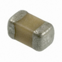
04025A101FAT2A AVX Corporation, 04025A101FAT2A Datasheet

04025A101FAT2A
Specifications of 04025A101FAT2A
Related parts for 04025A101FAT2A
04025A101FAT2A Summary of contents
Page 1
... C from -55°C to +125°C. Capacitance drift or hysteresis for C0G (NP0) ceramics is negligible at less than ±0.05% versus up to ±2% for films. Typical capacitance change with life is less than ±0.1% for C0G (NP0), one-fifth that shown by most other dielectrics ...
Page 2
C0G (NP0) Dielectric Specifications and Test Methods Parameter/Test Operating Temperature Range Capacitance Q Insulation Resistance Dielectric Strength Appearance Capacitance Resistance to Variation Flexure Q Stresses Insulation Resistance ≥ 95% of each terminal should be covered Solderability Appearance No defects, <25% ...
Page 3
C0G (NP0) Dielectric Capacitance Range PREFERRED SIZES ARE SHADED SIZE 0201 0402 Soldering Reflow Only Reflow Only Packaging All Paper All Paper MM 0.60 ± 0.03 1.00 ± 0.10 (L) Length (in.) (0.024 ± 0.001) (0.040 ± 0.004) MM 0.30 ...
Page 4
C0G (NP0) Dielectric Capacitance Range PREFERRED SIZES ARE SHADED SIZE 1210 Soldering Reflow Only Packaging Paper/Embossed MM 3.20 ± 0.20 (L) Length (in.) (0.126 ± 0.008) MM 2.50 ± 0.20 (W) Width (in.) (0.098 ± 0.008) MM 0.50 ± 0.25 ...
Page 5
Packaging of Chip Components Automatic Insertion Packaging TAPE & REEL QUANTITIES All tape and reel specifications are in compliance with RS481. Paper or Embossed Carrier Embossed Only Paper Only Qty. per Reel/7" Reel 2,000, 3,000 or 4,000, 10,000, 15,000 Contact ...
Page 6
Embossed Carrier Configuration 8 & 12mm Tape Only DEFORMATION BETWEEN EMBOSSMENTS A 0 TOP COVER B TAPE CENTER LINES S 1 MAX. CAVITY OF CAVITY SIZE - SEE NOTE 1 ...
Page 7
Paper Carrier Configuration 8 & 12mm Tape Only T BOTTOM TOP COVER COVER TAPE TAPE & 12mm Paper Tape Metric Dimensions Will Govern CONSTANT DIMENSIONS Tape Size +0.10 8mm 1.50 1.75 ± ...
Page 8
Bulk Case Packaging BENEFITS • Easier handling • Smaller packaging volume (1/20 of T/R packaging) • Easier inventory control • Flexibility • Recyclable CASE DIMENSIONS Shutter Slider 12mm 36mm 110mm Attachment Base CASE QUANTITIES Part Size 0402 Qty. 80,000 (pcs ...
Page 9
... XII. Power Loss (watts) Power Loss = (2 π fCV 2 XIII. KVA (Kilowatts) KVA = 2 π fCV - XIV. Temperature Characteristic (ppm/°C) Ct – – 25 XV. Cap Drift (%) C – C. 100 C 1 XVI. Reliability of Ceramic Capacitors ( ) ( XVII. Capacitors in Series (current the same) Any Number --- Two ...
Page 10
... General Description Basic Construction – A multilayer ceramic (MLC) capaci- tor is a monolithic block of ceramic containing two sets of offset, interleaved planar electrodes that extend to two opposite surfaces of the ceramic dielectric. This simple Ceramic Layer Formulations – Multilayer ceramic capacitors are available in both Class 1 and Class 2 formulations. Temperature ...
Page 11
General Description Table 1: EIA and MIL Temperature Stable and General Application Codes EIA CODE Percent Capacity Change Over Temperature Range RS198 Temperature Range X7 -55°C to +125°C X6 -55°C to +105°C X5 -55°C to +85°C Y5 -30°C to +85°C ...
Page 12
... A typical curve of aging rate for semi- stable ceramics is shown in Figure Class 2 ceramic capacitor that has been sitting on the shelf for a period of time, is heated above its curie point, (125°C for 4 hours or 150°C for 1 ⁄ ...
Page 13
... As a general statement, the piezoelectric output is higher, the higher the dielectric constant of the ceramic desirable to investigate this effect before using high “K” dielectrics as coupling capaci- tors in extremely low level applications. ...
Page 14
... Another important, often overlooked, reason for knowing the parasitic inductance is the calculation of the resonant frequency. This can be important for high frequency, by- pass capacitors, as the resonant point will give the most V signal attenuation. The resonant frequency is calculated from the simple equation: ...
Page 15
... Component Pad Design Component pads should be designed to achieve good solder filets and minimize component movement during reflow soldering. Pad designs are given below for the most common sizes of multilayer ceramic capacitors for both wave and reflow soldering. The basis of these designs is: WAVE SOLDERING D2 ...
Page 16
... The construction of the components is such that they will withstand the time/temperature profiles used in both wave and reflow soldering methods. Handling Chip multilayer ceramic capacitors should be handled with care to avoid damage or contamination from perspiration and skin oils. The use of tweezers or vacuum pick ups 200 ...
Page 17
... Ceramic capacitors are more susceptible to such stress because they don’t have compliant leads and are brittle in nature. The most frequent failure mode is low DC resistance or short circuit ...
Page 18
... Another common source of flexural stress is contact during parametric testing when test points are probed. If the PCB is allowed to flex during the test cycle, nearby ceramic capacitors may be broken. A third common source is board to board connections at vertical connectors where cables or other PCBs are con- nected to the PCB ...


