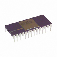
AD676BD Analog Devices Inc, AD676BD Datasheet - Page 3

AD676BD
Manufacturer Part Number
AD676BD
Description
ADC Single SAR 100KSPS 16-Bit Parallel 28-Pin SBCDIP
Manufacturer
Analog Devices Inc
Datasheet
1.AD676JNZ.pdf
(16 pages)
Specifications of AD676BD
Package
28SBCDIP
Resolution
16 Bit
Sampling Rate
100 KSPS
Architecture
SAR
Number Of Analog Inputs
1
Digital Interface Type
Parallel
Input Type
Voltage
Polarity Of Input Voltage
Bipolar
Rohs Status
RoHS non-compliant
Number Of Bits
16
Sampling Rate (per Second)
100k
Data Interface
Parallel
Number Of Converters
2
Power Dissipation (max)
480mW
Voltage Supply Source
Analog and Digital, Dual ±
Operating Temperature
-40°C ~ 85°C
Mounting Type
Through Hole
Package / Case
28-CDIP (0.600", 15.24mm)
For Use With
AD676-EB - BOARD EVAL SAMPLING ADC AD676
Lead Free Status / RoHS Status
Available stocks
Company
Part Number
Manufacturer
Quantity
Price
Part Number:
AD676BD
Manufacturer:
ADI/亚德诺
Quantity:
20 000
DC SPECIFICATIONS
Parameter
TEMPERATURE RANGE
ACCURACY
VOLTAGE REFERENCE INPUT RANGE
ANALOG INPUT
POWER SUPPLIES
NOTES
1
2
3
4
5
*For explanation of input characteristics, see “ANALOG INPUT” section.
Specifications subject to change without notice.
REV. A
V
Values shown apply to any temperature from T
Values shown are based upon calibration at +25 C with no additional calibration at temperature. Values shown are the worst case variation from the value at +25 C.
See “APPLICATIONS” section for recommended voltage reference circuit, and Figure 12 for dynamic performance with other reference voltage values.
See “APPLICATIONS” section for recommended input buffer circuit.
REF
J, K Grades
A, B Grades
Resolution
Integral Nonlinearity (INL)
Differential Nonlinearity (DNL)–No Missing Codes
Bipolar Zero Error
Gain Error (at Nominal Supplies)
Temperature Drift, Bipolar Zero
Temperature Drift, Gain
Input Range (V
Input Impedance
Input Settling Time
Input Capacitance During Sample
Aperture Delay
Aperture Jitter
Power Supply Rejection
Operating Current
Power Consumption
@ 83 kSPS, T
@ 100 kSPS, +25 C
@ 100 kSPS, T
@ 83 kSPS
@ 100 kSPS, +25 C
@ 100 kSPS
J, K Grades
A, B Grades
J, K Grades
A, B Grades
V
V
V
I
I
I
= 5.0 V, Conversion Rate = 83 kSPS unless otherwise noted. Values are post-calibration.
CC
EE
DD
CC
EE
DD
= –12 V
= +12 V
= +5 V
2
2
IN
MIN
5
10%
)
5%
MIN
5%
2
(at Nominal Supplies)
to T
to T
3
MAX
MAX
(T
MIN
3
to T
MIN
MAX
to T
, V
4
CC
MAX
(V
= +12 V
after calibration at that temperature.
REF
)
5%, V
Min
0
–40
16
5
EE
–3–
= –12 V
AD676J/A
Typ
16
0.005
0.005
0.005
0.01
0.0015
0.003
0.0015
0.003
*
2
6
100
14.5
14.5
2
360
1
1
2
1
1
1
5%, V
Max
+70
+85
10
50*
18
18
5
480
DD
V
REF
= +5 V
Min
0
–40
16
16
5
1O%)
1
AD676K/B
Typ
0.005
0.005
0.005
0.01
0.0015
0.003
0.0015
0.003
*
2
6
100
14.5
14.5
2
360
1
1
2
1
1
1
Max
+70
+85
10
50*
18
18
5
480
1.5
V
REF
Units
Bits
LSB
LSB
LSB
Bits
% FSR
% FSR
% FSR
% FSR
% FSR
% FSR
% FSR
% FSR
% FSR
V
V
pF
ns
ps
LSB
LSB
LSB
mA
mA
mA
mW
AD676
C
C
s


