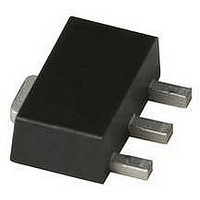
ATF-52189-BLK Avago Technologies US Inc., ATF-52189-BLK Datasheet - Page 3

ATF-52189-BLK
Manufacturer Part Number
ATF-52189-BLK
Description
IC PHEMT 2GHZ 4.5V 200MA SOT-89
Manufacturer
Avago Technologies US Inc.
Datasheet
1.ATF-52189-BLK.pdf
(18 pages)
Specifications of ATF-52189-BLK
Transistor Type
pHEMT FET
Frequency
2GHz
Gain
16dB
Voltage - Rated
7V
Current Rating
500mA
Noise Figure
1.5dB
Current - Test
200mA
Voltage - Test
4.5V
Power - Output
27dBm
Package / Case
SC-70-3, SOT-323-3
Drain Source Voltage Vds
7V
Continuous Drain Current Id
500mA
Power Dissipation Pd
1.5W
Noise Figure Typ
1.5dB
No. Of Pins
4
Peak Reflow Compatible (260 C)
Yes
No. Of Transistors
1
Current Gain-bandwidth Typ
6GHz
Marking, Smd
2Gx
Rohs Compliant
Yes
Current Gain-bandwidth Min
50MHz
Lead Free Status / RoHS Status
Lead free / RoHS Compliant
Available stocks
Company
Part Number
Manufacturer
Quantity
Price
Part Number:
ATF-52189-BLK
Manufacturer:
AVAGO/安华高
Quantity:
20 000
3
Symbol
PAE
ACLR
Notes:
1. Measurements at 2 GHz obtained using production test board described in Figure 1.
2. ACLR test spec is based on 3GPP TS 25.141 V5.3.1 (2002-06)
Input
Figure 1. Block diagram of the 2 GHz production test board used for NF, Gain, OIP3 , P1dB, PAE
and ACLR measurements. This circuit achieves a trade-off between optimal OIP3, P1dB and
VSWR. Circuit losses have been de-embedded from actual measurements.
Product Consistency Distribution Charts
Figure 4. Gain @ 2 GHz, 4.5V, 200 mA.
LSL = 14.8 dBm, Nominal = 16.1 dBm,
USL = 17.8 dB.
- Test Model 1
- Active Channels: PCCPCH + SCH + CPICH + PICH + SCCPCH + 64 DPCH (SF=128)
- Freq = 2140 MHz
- Pin = -8 dBm
- Channel Integrate Bandwidth = 3.84 MHz
Figure 2. OIP3 @ 2 GHz, 4.5V/200 mA.
LSL = 38.5 dBm, Nominal = 42.4 dBm.
150
120
150
120
90
60
30
90
60
30
0
0
15.5
–3 Std
Stdev=0.16
Stdev=0.35
–3 Std
41.5
Input Matching Circuit
Parameters and Test Conditions
Power Added Efficiency
Adjacent Channel Leakage
Power Ratio
Γ_ang=-131.3°
Γ_mag=0.76
16
42
GAIN (dBm)
OIP3 (dBm)
42.5
[1,2]
16.5
43
+3 Std
+3 Std
43.5
17
DUT
[1,2]
Figure 3. P1dB @ 2 GHz, 4.5V, 200 mA.
LSL = 25.5 dBm, Nominal = 27.1 dBm.
Figure 5. NF @ 2 GHz, 4.5V, 200 mA.
Nominal = 1.5 dBm.
150
120
150
120
90
60
30
90
60
30
0
0
1
Output Matching Circuit
Stdev=0.30
Stdev=0.10
26.25
–3 Std
–3 Std
f=900 MHz
f=2.0 GHz
f=2.4 GHz
Offset BW = 5 MHz
Offset BW = 10 MHz
Γ_ang=-176.6°
1.25
Γ_mag=0.32
26.75
P1dB (dBm)
NF (dBm)
1.5
27.25
1.75
27.75
+3 Std
+3 Std
28.25
2
Output
Units
%
%
%
dBc
dBc
Notes:
1. Distribution data sample size is 500 samples
2. Measurements are made on production test
taken from 3 different wafers. Future wafers
allocated to this product may have nominal
values anywhere between the upper and
lower limits.
board, which represents a trade-off between
optimal OIP3, P1dB and VSWR. Circuit losses
have been de-embedded from actual
measurements.
Min.
—
40.0
—
—
—
Typ.
50.0
55.0
52.0
-58.0
-66.0
Max.
—
—
—
—


