MCR718T4G ON Semiconductor, MCR718T4G Datasheet - Page 2
MCR718T4G
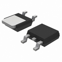
Manufacturer Part Number
MCR718T4G
Description
THYRISTOR SCR 4A 600V DPAK
Manufacturer
ON Semiconductor
Datasheet
1.MCR716T4G.pdf
(5 pages)
Specifications of MCR718T4G
Scr Type
Sensitive Gate
Voltage - Off State
600V
Voltage - Gate Trigger (vgt) (max)
800mV
Voltage - On State (vtm) (max)
2.2V
Current - On State (it (av)) (max)
2.6A
Current - On State (it (rms)) (max)
4A
Current - Gate Trigger (igt) (max)
75µA
Current - Hold (ih) (max)
5mA
Current - Off State (max)
10µA
Current - Non Rep. Surge 50, 60hz (itsm)
25A @ 60Hz
Operating Temperature
-40°C ~ 110°C
Mounting Type
Surface Mount
Package / Case
DPak, TO-252 (2 leads+tab), SC-63
Current - On State (it (rms) (max)
4A
Lead Free Status / RoHS Status
Lead free / RoHS Compliant
Other names
MCR718T4GOS
MCR718T4GOS
MCR718T4GOSTR
MCR718T4GOS
MCR718T4GOSTR
Available stocks
Company
Part Number
Manufacturer
Quantity
Price
Company:

Part Number:
MCR718T4G
Manufacturer:
ON Semiconductor
Quantity:
6 000
Company:
Part Number:
MCR718T4G
Manufacturer:
ON
Quantity:
12 500
Part Number:
MCR718T4G
Manufacturer:
ON/安森美
Quantity:
20 000


2. Case 369C, when surface mounted on minimum recommended pad size.
3. Ratings apply for negative gate voltage or R
4. Pulse Test: Pulse Width ≤ 2 ms, Duty Cycle ≤ 2%.
5. R
†For information on tape and reel specifications, including part orientation and tape sizes, please refer to our Tape and Reel Packaging
THERMAL CHARACTERISTICS
ELECTRICAL CHARACTERISTICS
OFF CHARACTERISTICS
ON CHARACTERISTICS
DYNAMIC CHARACTERISTICS
ORDERING INFORMATION
Specifications Brochure, BRD8011/D.
MCR716T4
MCR716T4G
MCR718T4
MCR718T4G
Thermal Resistance, Junction−to−Case
Thermal Resistance, Junction−to−Ambient (Note 2)
Maximum Lead Temperature for Soldering Purposes 1/8″ from Case for 10 Seconds
Peak Repetitive Forward or Reverse Blocking Current; R
Peak Reverse Gate Blocking Voltage (I
Peak Reverse Gate Blocking Current (V
Peak Forward On−State Voltage (Note 4)
Gate Trigger Current (Continuous dc) (Note 5)
Gate Trigger Voltage (Continuous dc) (Note 5)
Holding Current (Note 3)
Latching Current (Note 3) (R
Total Turn-On Time
Critical Rate of Rise of Off−State Voltage
Repetitive Critical Rate of Rise of On−State Current
on the anode. Devices should not be tested with a constant current source for forward and reverse blocking capability such that the voltage
applied exceeds the rated blocking voltage.
(V
(I
(I
(V
(V
(V
(V
(V
(Source Voltage = 12 V, R
(V
(V
(f = 60 Hz, I
GK
TM
TM
AK
D
D
D
D
D
D
D
current not included in measurements.
= 12 Vdc, R
= 12 Vdc, R
= 12 Vdc, Initiating Current = 20 mA, R
= 12 Vdc, I
= 12 Vdc, I
= Rated V
= 0.67 x Rated V
= 5.0 A Peak)
= 8.2 A Peak)
= Rated V
PK
DRM
= 30 A, PW = 100 ms, dIG/dt = 1 A/ms)
G
G
DRM
L
L
= 2.0 mA, T
= 2.0 mA, T
Device
= 30 W)
= 30 W)
, Rise Time = 20 ns, Pulse Width = 10 ms)
or V
DRM
RRM
, R
GK
S
= 6 kW, I
GK
)
C
C
= 1 kW)
= 25°C)
= −40°C)
Characteristic
Characteristic
= 1 kW, Exponential Waveform, T
T
GR
GR
(T
= 8 A(pk), R
C
= 10 mA)
= 10 V)
= 25°C unless otherwise noted.)
GK
GK
= 1 kW. Devices shall not have a positive gate voltage concurrently with a negative voltage
= 1 kW)
GK
= 1 kW)
http://onsemi.com
GK
= 1 kW (Note 3)
T
T
T
T
T
T
T
T
T
C
C
C
C
C
C
C
C
C
= 25°C
= 110°C
= 25°C
= −40°C
= 25°C
= −40°C
= 110°C
= 25°C
= −40°C
(Pb−Free)
(Pb−Free)
Package
DPAK
DPAK
DPAK
DPAK
2
J
= 110°C)
Symbol
Symbol
V
R
I
I
I
dv/dt
R
V
di/dt
V
DRM
RRM
RGM
I
RGM
T
t
GT
I
qJC
qJA
I
TM
GT
gt
H
L
L
2500 / Tape and Reel
Min
1.0
0.3
0.2
0.4
5.0
10
−
−
−
−
−
−
−
−
−
−
−
−
Shipping
Max
12.5
0.55
260
Typ
3.0
1.3
1.5
1.0
2.0
80
25
10
−
−
−
−
−
−
−
−
−
−
†
Max
200
300
100
1.2
1.5
2.2
0.8
1.0
5.0
5.0
5.0
10
18
75
10
10
−
−
°C/W
°C/W
V/ms
A/ms
Unit
Unit
mA
mA
°C
mA
mA
mA
ms
V
V
V
Related parts for MCR718T4G
Image
Part Number
Description
Manufacturer
Datasheet
Request
R

Part Number:
Description:
ON Semiconductor [VOLTAGE REGULATOR]
Manufacturer:
ON Semiconductor
Datasheet:
Part Number:
Description:
357-036-542-201 CARDEDGE 36POS DL .156 BLK LOPRO
Manufacturer:
ON Semiconductor
Datasheet:
Part Number:
Description:
357-036-542-201 CARDEDGE 36POS DL .156 BLK LOPRO
Manufacturer:
ON Semiconductor
Datasheet:
Part Number:
Description:
357-036-542-201 CARDEDGE 36POS DL .156 BLK LOPRO
Manufacturer:
ON Semiconductor
Datasheet:
Part Number:
Description:
357-036-542-201 CARDEDGE 36POS DL .156 BLK LOPRO
Manufacturer:
ON Semiconductor
Datasheet:
Part Number:
Description:
357-036-542-201 CARDEDGE 36POS DL .156 BLK LOPRO
Manufacturer:
ON Semiconductor
Datasheet:
Part Number:
Description:
357-036-542-201 CARDEDGE 36POS DL .156 BLK LOPRO
Manufacturer:
ON Semiconductor
Datasheet:
Part Number:
Description:
357-036-542-201 CARDEDGE 36POS DL .156 BLK LOPRO
Manufacturer:
ON Semiconductor
Datasheet:
Part Number:
Description:
357-036-542-201 CARDEDGE 36POS DL .156 BLK LOPRO
Manufacturer:
ON Semiconductor
Datasheet:
Part Number:
Description:
357-036-542-201 CARDEDGE 36POS DL .156 BLK LOPRO
Manufacturer:
ON Semiconductor
Datasheet:
Part Number:
Description:
357-036-542-201 CARDEDGE 36POS DL .156 BLK LOPRO
Manufacturer:
ON Semiconductor
Datasheet:
Part Number:
Description:
Manufacturer:
ON Semiconductor
Datasheet:
Part Number:
Description:
Manufacturer:
ON Semiconductor
Datasheet:
Part Number:
Description:
Manufacturer:
ON Semiconductor
Datasheet: