MCR8DCNT4G ON Semiconductor, MCR8DCNT4G Datasheet

THYRISTOR SCR 8A 800V DPAK-4

MCR8DCNT4G

Manufacturer Part Number
MCR8DCNT4G
Description
THYRISTOR SCR 8A 800V DPAK-4
Manufacturer
ON Semiconductor
Datasheet

Specifications of MCR8DCNT4G

Scr Type
Standard Recovery
Voltage - Off State
800V
Voltage - Gate Trigger (vgt) (max)
1V
Voltage - On State (vtm) (max)
1.8V
Current - On State (it (av)) (max)
5.1A
Current - On State (it (rms)) (max)
8A
Current - Gate Trigger (igt) (max)
15mA
Current - Hold (ih) (max)
30mA
Current - Off State (max)
10µA
Current - Non Rep. Surge 50, 60hz (itsm)
80A @ 60Hz
Operating Temperature
-40°C ~ 125°C
Mounting Type
Surface Mount
Package / Case
DPak, TO-252 (2 leads+tab), SC-63
Current - On State (it (rms) (max)
8A
Breakover Current Ibo Max
80 A
Rated Repetitive Off-state Voltage Vdrm
800 V
Off-state Leakage Current @ Vdrm Idrm
0.01 mA
Forward Voltage Drop
1.8 V
Gate Trigger Voltage (vgt)
1 V
Gate Trigger Current (igt)
15 mA
Holding Current (ih Max)
30 mA
Mounting Style
SMD/SMT
Lead Free Status / RoHS Status
Lead free / RoHS Compliant
Other names
MCR8DCNT4G
MCR8DCNT4GOSTR

Available stocks

Company
Part Number
Manufacturer
Quantity
Price
Part Number:
MCR8DCNT4G
Manufacturer:
ON
Quantity:
12 500
Part Number:
MCR8DCNT4G
Manufacturer:
ON/安森美
Quantity:
20 000
MCR8DCM, MCR8DCN
Silicon Controlled Rectifiers
Reverse Blocking Thyristors
applications such as motor control; process control; temperature, light
and speed control.
Features
Maximum ratings are those values beyond which device damage can occur.
Maximum ratings applied to the device are individual stress limit values (not
normal operating conditions) and are not valid simultaneously. If these limits are
exceeded, device functional operation is not implied, damage may occur and
reliability may be affected.
1. V
MAXIMUM RATINGS
© Semiconductor Components Industries, LLC, 2005
November, 2005 − Rev. 4
Peak Repetitive Off−State Voltage
(Note 1) (T
50 to 60 Hz, Gate Open)
On−State RMS Current
(180° Conduction Angles; T
Average On−State Current
(180° Conduction Angles; T
Peak Non-Repetitive Surge Current
(1/2 Cycle, Sine Wave 60 Hz, T
Circuit Fusing Consideration (t = 8.3 msec)
Forward Peak Gate Power
(Pulse Width ≤ 1.0 msec, T
Forward Average Gate Power
(t = 8.3 msec, T
Forward Peak Gate Current
(Pulse Width ≤ 1.0 msec, T
Operating Junction Temperature Range
Storage Temperature Range
Designed for high volume, low cost, industrial and consumer
Small Size
Passivated Die for Reliability and Uniformity
Low Level Triggering and Holding Characteristics
Available in Surface Mount Lead Form − Case 369C
Epoxy Meets UL 94 V−0 @ 0.125 in
ESD Ratings:
Pb−Free Packages are Available
for zero or negative gate voltage; positive gate voltage shall not be applied
concurrent with negative potential on the anode. Blocking voltages shall not
be tested with a constant current source such that the voltage ratings of the
device are exceeded.
DRM
, V
RRM
J
= −40 to 125°C, Sine Wave,
for all types can be applied on a continuous basis. Ratings apply
C
Rating
= 105°C)
Machine Model, C u 400 V
Human Body Model, 3B u 8000 V
(T
J
C
C
MCR8DCM
MCR8DCN
= 25°C unless otherwise noted)
C
C
= 105°C)
= 105°C)
Preferred Device
= 105°C)
= 105°C)
J
= 125°C)
Symbol
I
P
V
V
T(RMS)
I
I
P
T(AV)
I
T
G(AV)
DRM,
TSM
RRM
I
GM
T
GM
stg
2
J
t
−40 to 125
−40 to 150
Value
600
800
8.0
5.1
5.0
0.5
2.0
80
26
1
A
Unit
2
°C
°C
W
W
V
A
A
A
A
sec
See detailed ordering and shipping information in the package
dimensions section on page 2 of this data sheet.
Preferred devices are recommended choices for future use
and best overall value.
1
2
3
4
Y
WW
CR8DCx
G
ORDERING INFORMATION
8 AMPERES RMS
600 − 800 VOLTS
A
MARKING DIAGRAM
http://onsemi.com
PIN ASSIGNMENT
1 2
CASE 369C
= Year
= Work Week
= Device Code
= Pb−Free Package
STYLE 4
SCRs
DPAK
8DCxG
x= M or N
YWW
3
Publication Order Number:
CR
Cathode
Anode
Anode
Gate
4
G
K
MCR8DCM/D

Related parts for MCR8DCNT4G

MCR8DCNT4G Summary of contents

Page 1

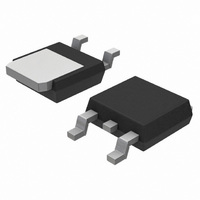
MCR8DCM, MCR8DCN Preferred Device Silicon Controlled Rectifiers Reverse Blocking Thyristors Designed for high volume, low cost, industrial and consumer applications such as motor control; process control; temperature, light and speed control. Features • Small Size • Passivated Die for Reliability ...

Page 2

... Pulse Test: Pulse Width ≤ 2.0 ms, Duty Cycle ≤ 2%. ORDERING INFORMATION Device MCR8DCMT4 MCR8DCMT4G MCR8DCNT4 MCR8DCNT4G †For information on tape and reel specifications, including part orientation and tape sizes, please refer to our Tape and Reel Packaging Specifications Brochure, BRD8011/D. MCR8DCM, MCR8DCN 2 25° ...

Page 3

Voltage Current Characteristic of SCR Symbol Parameter V Peak Repetitive Off State Forward Voltage DRM I Peak Forward Blocking Current DRM V Peak Repetitive Off State Reverse Voltage RRM I Peak Reverse Blocking Current RRM V Peak On State Voltage ...

Page 4

T , JUNCTION TEMPERATURE (°C) J Figure 5. Typical Gate Trigger Current versus Junction Temperature 100 10 1.0 −40 −25 −10 5 JUNCTION ...

Page 5

... G 0.13 (0.005) *For additional information on our Pb−Free strategy and soldering details, please download the ON Semiconductor Soldering and Mounting Techniques Reference Manual, SOLDERRM/D. ON Semiconductor and are registered trademarks of Semiconductor Components Industries, LLC (SCILLC). SCILLC reserves the right to make changes without further notice to any products herein ...

Related keywords