EMZ1DXV6T5G ON Semiconductor, EMZ1DXV6T5G Datasheet

TRANS NPN GP/PNP DUAL SOT-563

EMZ1DXV6T5G

Manufacturer Part Number
EMZ1DXV6T5G
Description
TRANS NPN GP/PNP DUAL SOT-563
Manufacturer
ON Semiconductor
Datasheet

Specifications of EMZ1DXV6T5G

Transistor Type
NPN, PNP
Current - Collector (ic) (max)
100mA
Voltage - Collector Emitter Breakdown (max)
60V
Vce Saturation (max) @ Ib, Ic
400mV @ 5mA, 50mA / 500mV @ 5mA, 50mA
Dc Current Gain (hfe) (min) @ Ic, Vce
120 @ 1mA, 6V
Power - Max
500mW
Frequency - Transition
180MHz, 140MHz
Mounting Type
Surface Mount
Package / Case
SOT-563, SOT-6
Lead Free Status / RoHS Status
Lead free / RoHS Compliant
Current - Collector Cutoff (max)
-

Available stocks

Company
Part Number
Manufacturer
Quantity
Price
Part Number:
EMZ1DXV6T5G
Manufacturer:
ON
Quantity:
30 000
EMZ1DXV6T1,
EMZ1DXV6T5
Dual General Purpose
Transistors
NPN/PNP Dual (Complementary)
applications. It is housed in the SOT−563 which is designed for low
power surface mount applications.
Features
Stresses exceeding Maximum Ratings may damage the device. Maximum
Ratings are stress ratings only. Functional operation above the Recommended
Operating Conditions is not implied. Extended exposure to stresses above the
Recommended Operating Conditions may affect device reliability.
1. FR−4 @ Minimum Pad.
© Semiconductor Components Industries, LLC, 2006
April, 2006 − Rev. 1
MAXIMUM RATINGS
THERMAL CHARACTERISTICS
Collector −Emitter Voltage
Collector −Base Voltage
Emitter −Base Voltage
Collector Current − Continuous
Total Device Dissipation
Thermal Resistance,
Total Device Dissipation
Thermal Resistance,
Junction and Storage
This transistor is designed for general purpose amplifier
Lead−Free Solder Plating
Low V
These are Pb−Free Devices
Junction-to-Ambient
Junction-to-Ambient
Temperature Range
T
Derate above 25°C
T
Derate above 25°C
A
A
(Both Junctions Heated)
(One Junction Heated)
= 25°C
= 25°C
CE(SAT)
Characteristic
Characteristic
Rating
, t0.5 V
Symbol
Symbol
Symbol
T
V
V
V
R
R
J
P
P
CEO
CBO
, T
EBO
I
qJA
qJA
C
D
D
stg
357 (Note 1)
500 (Note 1)
−55 to +150
2.9 (Note 1)
4.0 (Note 1)
(Note 1)
(Note 1)
Value
−100
−6.0
Max
Max
−60
−50
350
250
1
mW/°C
mW/°C
mAdc
°C/W
°C/W
Unit
Unit
Unit
mW
mW
°C
V
V
V
See detailed ordering and shipping information in the package
dimensions section on page 2 of this data sheet.
(Note: Microdot may be in either location)
Q
ORDERING INFORMATION
(3)
(4)
1
3Z = Specific Device Code
M
G
MARKING DIAGRAM
http://onsemi.com
= Month Code
= Pb−Free Package
6
CASE 463A
SOT−563
STYLE 1
3Z M G
(5)
Publication Order Number:
G
1
(2)
EMZ1DXV6/D
(1)
(6)
Q
2

Related parts for EMZ1DXV6T5G

EMZ1DXV6T5G Summary of contents

Page 1

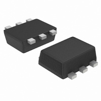
EMZ1DXV6T1, EMZ1DXV6T5 Dual General Purpose Transistors NPN/PNP Dual (Complementary) This transistor is designed for general purpose amplifier applications housed in the SOT−563 which is designed for low power surface mount applications. Features • Lead−Free Solder Plating • , ...

Page 2

... Device mounted on a FR-4 glass epoxy printed circuit board using the minimum recommended footprint. ORDERING INFORMATION Device EMZ1DXV6T1 EMZ1DXV6T1G EMZ1DXV6T5 EMZ1DXV6T5G †For information on tape and reel specifications, including part orientation and tape sizes, please refer to our Tape and Reel Packaging Specifications Brochure, BRD8011/D. *This package is inherently Pb−Free. EMZ1DXV6T1, EMZ1DXV6T5 (T = 25° ...

Page 3

TYPICAL ELECTRICAL CHARACTERISTICS − Q1, PNP T = 25°C A 120 COLLECTOR VOLTAGE (V) CE Figure 1. I − 1.5 1 0.5 0 0.01 0.1 1 ...

Page 4

TYPICAL ELECTRICAL CHARACTERISTICS − Q2, NPN 25° COLLECTOR VOLTAGE (V) CE Figure 1. I − 1.5 1 0.5 0 0.01 0.1 ...

Page 5

... M *For additional information on our Pb−Free strategy and soldering details, please download the ON Semiconductor Soldering and Mounting Techniques Reference Manual, SOLDERRM/D. ON Semiconductor and are registered trademarks of Semiconductor Components Industries, LLC (SCILLC). SCILLC reserves the right to make changes without further notice to any products herein ...

Related keywords