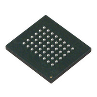
XC2C64A-7CPG56I Xilinx Inc, XC2C64A-7CPG56I Datasheet - Page 8

XC2C64A-7CPG56I
Manufacturer Part Number
XC2C64A-7CPG56I
Description
CPLD CoolRunner™-II Family 1.5K Gates 64 Macro Cells 159MHz 0.18um (CMOS) Technology 1.8V 56-Pin CSBGA
Manufacturer
Xilinx Inc
Series
CoolRunner IIr
Specifications of XC2C64A-7CPG56I
Package
56CSBGA
Family Name
CoolRunnerÂ-II
Device System Gates
1500
Number Of Macro Cells
64
Maximum Propagation Delay Time
7.5 ns
Number Of User I/os
45
Number Of Logic Blocks/elements
4
Typical Operating Supply Voltage
1.8 V
Maximum Operating Frequency
159 MHz
Number Of Product Terms Per Macro
40
Operating Temperature
-40 to 85 °C
Features
Programmable
Package / Case
56-CSBGA
Mounting Type
Surface Mount
Voltage
1.8V
Number Of I /o
45
Memory Type
CMOS
Programmable Type
In System Programmable
Number Of Macrocells
64
Delay Time Tpd(1) Max
6.7ns
Voltage Supply - Internal
1.7 V ~ 1.9 V
Number Of Logic Elements/blocks
4
Number Of Gates
1500
Lead Free Status / RoHS Status
Lead free / RoHS Compliant
Number Of Logic Elements/cells
-
Lead Free Status / Rohs Status
Lead free / RoHS Compliant
For Use With
122-1536 - KIT STARTER SPARTAN-3E122-1532 - KIT DEVELOPMENT SPARTAN 3ADSP
Lead Free Status / RoHS Status
Lead free / RoHS Compliant
Available stocks
Company
Part Number
Manufacturer
Quantity
Price
Company:
Part Number:
XC2C64A-7CPG56I
Manufacturer:
XILINX
Quantity:
440
Part Number:
XC2C64A-7CPG56I
Manufacturer:
XILINX/赛灵思
Quantity:
20 000
CoolRunner-II CPLD Family
nally generated DataGATE control logic can be assigned to
this I/O pin with the BUFG=DATA_GATE attribute.
Global Signals
Global signals, clocks (GCK), sets/resets (GSR), and output
enables (GTS), are designed to strongly resemble each
other. This approach enables design software to make the
best utilization of their capabilities. Each global capability is
supplemented by a corresponding product term version.
Figure 7
trees. The pin input is buffered, then drives multiple internal
global signal traces to deliver low skew and reduce loading
delays. GCK, GSR, and GTS can also be used as general
8
shows the common structure of the global signal
Figure 6: DataGATE Architecture (output drivers not shown)
Latch
Latch
To AIM
To AIM
MC16
MC16
MC1
MC2
MC1
MC2
PLA
PLA
DataGATE Assertion Rail
www.xilinx.com
AIM
purpose I/Os if they are not needed as global signals. The
DataGATE assertion rail is also a global signal.
Figure 7: Global Clocks (GCK), Sets/Resets (GSR), and
PLA
PLA
MC16
MC16
MC1
MC2
MC1
MC2
Output Enables (GTS)
To AIM
To AIM
To AIM
DS090 (v3.1) September 11, 2008
Latch
Latch
Latch
DS090_07_101001
Product Specification
DS090_06_111201
R


