XC2S100E-6PQG208C Xilinx Inc, XC2S100E-6PQG208C Datasheet - Page 4
XC2S100E-6PQG208C
Manufacturer Part Number
XC2S100E-6PQG208C
Description
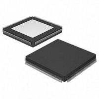
FPGA Spartan®-IIE Family 100K Gates 2700 Cells 357MHz 0.15um Technology 1.8V 208-Pin PQFP
Manufacturer
Xilinx Inc
Series
Spartan™-IIEr
Datasheet
1.XC2S50E-6TQG144C.pdf
(108 pages)
Specifications of XC2S100E-6PQG208C
Package
208PQFP
Family Name
Spartan®-IIE
Device Logic Cells
2700
Device Logic Units
600
Device System Gates
100000
Maximum Internal Frequency
357 MHz
Typical Operating Supply Voltage
1.8 V
Maximum Number Of User I/os
146
Ram Bits
40960
Number Of Logic Elements/cells
2700
Number Of Labs/clbs
600
Total Ram Bits
40960
Number Of I /o
146
Number Of Gates
100000
Voltage - Supply
1.71 V ~ 1.89 V
Mounting Type
Surface Mount
Operating Temperature
0°C ~ 85°C
Package / Case
208-BFQFP
Lead Free Status / RoHS Status
Lead free / RoHS Compliant
Available stocks
Company
Part Number
Manufacturer
Quantity
Price
Company:

Part Number:
XC2S100E-6PQG208C
Manufacturer:
CMD
Quantity:
9 282
Company:
Part Number:
XC2S100E-6PQG208C
Manufacturer:
XILINX
Quantity:
855
Company:
Part Number:
XC2S100E-6PQG208C
Manufacturer:
Xilinx Inc
Quantity:
10 000


Spartan-IIE FPGA Family: Introduction and Ordering Information
General Overview
The Spartan-IIE family of FPGAs have a regular, flexible,
programmable architecture of Configurable Logic Blocks
(CLBs), surrounded by a perimeter of programmable
Input/Output Blocks (IOBs). There are four Delay-Locked
Loops (DLLs), one at each corner of the die. Two columns
of block RAM lie on opposite sides of the die, between the
CLBs and the IOB columns. The XC2S400E has four col-
umns and the XC2S600E has six columns of block RAM.
These functional elements are interconnected by a powerful
hierarchy of versatile routing channels (see
Spartan-IIE FPGAs are customized by loading configura-
tion data into internal static memory cells. Unlimited repro-
gramming cycles are possible with this approach. Stored
values in these cells determine logic functions and intercon-
nections implemented in the FPGA. Configuration data can
be read from an external serial PROM (master serial mode),
or written into the FPGA in slave serial, slave parallel, or
Boundary Scan modes. Xilinx offers multiple types of
low-cost configuration solutions including the Platform
Flash in-system programmable configuration PROMs.
Spartan-IIE FPGAs are typically used in high-volume appli-
cations where the versatility of a fast programmable solution
adds benefits. Spartan-IIE FPGAs are ideal for shortening
product development cycles while offering a cost-effective
solution for high volume production.
4
I/O LOGIC
DLL
DLL
Figure 1: Basic Spartan-IIE Family FPGA Block Diagram
Figure
CLBs
CLBs
1).
www.xilinx.com
Spartan-IIE FPGAs achieve high-performance, low-cost
operation through advanced architecture and semiconduc-
tor technology. Spartan-IIE devices provide system clock
rates beyond 200 MHz. In addition to the conventional ben-
efits of high-volume programmable logic solutions, Spar-
tan-IIE FPGAs also offer on-chip synchronous single-port
and dual-port RAM (block and distributed form), DLL clock
drivers, programmable set and reset on all flip-flops, fast
carry logic, and many other features.
Spartan-IIE Family Compared to Spartan-II
Family
•
•
•
•
•
•
•
Higher density and more I/O
Higher performance
Unique pinouts in cost-effective packages
Differential signaling
-
V
-
-
-
PCI, LVTTL, and LVCMOS2 input buffers powered by
V
Unique larger bitstream
CCINT
CCO
CLBs
CLBs
LVDS, Bus LVDS, LVPECL
Lower power
5V tolerance with external resistor
3V tolerance directly
instead of V
= 1.8V
CCINT
DLL
DLL
DS077_01_052102
DS077-1 (v2.3) June 18, 2008
Product Specification
R
Related parts for XC2S100E-6PQG208C
Image
Part Number
Description
Manufacturer
Datasheet
Request
R

Part Number:
Description:
FPGA Spartan®-IIE Family 100K Gates 2700 Cells 357MHz 0.15um Technology 1.8V 256-Pin FTBGA
Manufacturer:
Xilinx Inc
Datasheet:

Part Number:
Description:
FPGA Spartan®-IIE Family 100K Gates 2700 Cells 357MHz 0.15um Technology 1.8V 256-Pin FTBGA
Manufacturer:
Xilinx Inc
Datasheet:
Part Number:
Description:
FPGA Spartan®-IIE Family 100K Gates 2700 Cells 357MHz 0.15um Technology 1.8V 256-Pin FTBGA
Manufacturer:
Xilinx Inc
Datasheet:

Part Number:
Description:
FPGA Spartan®-IIE Family 100K Gates 2700 Cells 357MHz 0.15um Technology 1.8V 208-Pin PQFP
Manufacturer:
Xilinx Inc
Datasheet:
Part Number:
Description:
FPGA Spartan®-IIE Family 100K Gates 2700 Cells 357MHz 0.15um Technology 1.8V 208-Pin PQFP
Manufacturer:
Xilinx Inc
Datasheet:

Part Number:
Description:
FPGA Spartan®-IIE Family 100K Gates 2700 Cells 357MHz 0.15um Technology 1.8V 144-Pin TQFP
Manufacturer:
Xilinx Inc
Datasheet:
Part Number:
Description:
FPGA Spartan®-IIE Family 100K Gates 2700 Cells 357MHz 0.15um Technology 1.8V 144-Pin TQFP
Manufacturer:
Xilinx Inc
Datasheet:
Part Number:
Description:
FPGA Spartan®-IIE Family 100K Gates 2700 Cells 357MHz 0.15um Technology 1.8V 456-Pin FBGA
Manufacturer:
Xilinx Inc
Datasheet:
Part Number:
Description:
FPGA Spartan®-IIE Family 100K Gates 2700 Cells 357MHz 0.15um Technology 1.8V 256-Pin FTBGA
Manufacturer:
Xilinx Inc
Datasheet:
Part Number:
Description:
Spartan-IIE FPGA
Manufacturer:
XILINX [Xilinx, Inc]
Datasheet:
Part Number:
Description:
Spartan-IIE 1.8V FPGA Family
Manufacturer:
XILINX [Xilinx, Inc]
Datasheet:
Part Number:
Description:
FPGA Spartan®-IIE Family 100K Gates 2700 Cells 357MHz 0.15um Technology 1.8V 144-Pin TQFP
Manufacturer:
Xilinx Inc
Datasheet:
Part Number:
Description:
FPGA Spartan®-IIE Family 100K Gates 2700 Cells 357MHz 0.15um Technology 1.8V 144-Pin TQFP
Manufacturer:
Xilinx Inc
Datasheet:
Part Number:
Description:
FPGA Spartan®-IIE Family 100K Gates 2700 Cells 400MHz 0.15um Technology 1.8V 144-Pin TQFP
Manufacturer:
Xilinx Inc
Datasheet:
Part Number:
Description:
FPGA Spartan®-IIE Family 100K Gates 2700 Cells 400MHz 0.15um Technology 1.8V 208-Pin PQFP
Manufacturer:
Xilinx Inc
Datasheet: