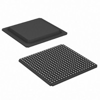
XC3S1600E-5FGG400C Xilinx Inc, XC3S1600E-5FGG400C Datasheet - Page 147

XC3S1600E-5FGG400C
Manufacturer Part Number
XC3S1600E-5FGG400C
Description
FPGA Spartan®-3E Family 1.6M Gates 33192 Cells 657MHz 90nm (CMOS) Technology 1.2V 400-Pin FBGA
Manufacturer
Xilinx Inc
Series
Spartan™-3Er
Datasheet
1.XC3S100E-4VQG100C.pdf
(233 pages)
Specifications of XC3S1600E-5FGG400C
Package
400FBGA
Family Name
Spartan®-3E
Device Logic Cells
33192
Device Logic Units
3688
Device System Gates
1600000
Number Of Registers
29504
Maximum Internal Frequency
657 MHz
Typical Operating Supply Voltage
1.2 V
Maximum Number Of User I/os
304
Ram Bits
663552
Number Of Logic Elements/cells
33192
Number Of Labs/clbs
3688
Total Ram Bits
663552
Number Of I /o
304
Number Of Gates
1600000
Voltage - Supply
1.14 V ~ 1.26 V
Mounting Type
Surface Mount
Operating Temperature
0°C ~ 85°C
Package / Case
400-BGA
Lead Free Status / RoHS Status
Lead free / RoHS Compliant
For Use With
HW-XA3S1600E-UNI-G - KIT DEVELOPMENT AUTOMOTIVE ECU
Lead Free Status / RoHS Status
Lead free / RoHS Compliant
Available stocks
Company
Part Number
Manufacturer
Quantity
Price
Company:
Part Number:
XC3S1600E-5FGG400C
Manufacturer:
XILINX
Quantity:
259
Company:
Part Number:
XC3S1600E-5FGG400C
Manufacturer:
Xilinx Inc
Quantity:
10 000
Part Number:
XC3S1600E-5FGG400C
Manufacturer:
XILINX/赛灵思
Quantity:
20 000
Table 107: Switching Characteristics for the DFS (Continued)
Notes:
1.
2.
3.
4.
5.
6.
Phase Shifter (PS)
Table 108: Recommended Operating Conditions for the PS in Variable Phase Mode
Table 109: Switching Characteristics for the PS in Variable Phase Mode
DS312-3 (v3.8) August 26, 2009
Product Specification
Lock Time
LOCK_FX
Phase Shifting Range
MAX_STEPS
FINE_SHIFT_RANGE_MIN
FINE_SHIFT_RANGE_MAX
Operating Frequency Ranges
PSCLK_FREQ
(F
Input Pulse Requirements
PSCLK_PULSE
PSCLK
The numbers in this table are based on the operating conditions set forth in
For optimal jitter tolerance and faster lock time, use the CLKIN_PERIOD attribute.
Maximum output jitter is characterized within a reasonable noise environment (150 ps input period jitter, 40 SSOs and 25% CLB
switching). Output jitter strongly depends on the environment, including the number of SSOs, the output drive strength, CLB
utilization, CLB switching activities, switching frequency, power supply and PCB design. The actual maximum output jitter depends on
the system application.
The CLKFX and CLKFX180 outputs always have an approximate 50% duty cycle.
Some duty-cycle and alignment specifications include 1% of the CLKFX output period or 0.01 UI. Example: The data sheet specifies
a maximum jitter of "±[1% of CLKFX period + 300]". Assume the CLKFX output frequency is 100 MHz. The equivalent CLKFX period
is 10 ns and 1% of 10 ns is 0.1 ns or 100 ps. According to the data sheet, the maximum jitter is ±[100 ps + 300 ps] = ±400 ps.
Use the Spartan-3A Jitter Calculator (www.xilinx.com/support/documentation/data_sheets/s3a_jitter_calc.zip) to estimate DFS output jitter.
Use the Clocking Wizard to determine jitter for a specific design.
Symbol
)
(2)
Symbol
Symbol
R
(2)
Frequency for the PSCLK input
PSCLK pulse width as a percentage of the PSCLK period
The time from deassertion at the DCM’s
Reset input to the rising transition at its
LOCKED output. The DFS asserts
LOCKED when the CLKFX and
CLKFX180 signals are valid. If using
both the DLL and the DFS, use the
longer locking time.
Maximum allowed number of DCM_DELAY_STEP
steps for a given CLKIN clock period, where T = CLKIN
clock period in ns. If using
CLKIN_DIVIDE_BY_2 = TRUE, double the effective
clock period.
Minimum guaranteed delay for variable phase shifting
Maximum guaranteed delay for variable phase shifting
Description
Description
Description
www.xilinx.com
F
F
5 MHz <
15 MHz
15 MHz
CLKIN
CLKIN
<
>
Table 77
Device
All
and
40%
CLKIN < 60 MHz
CLKIN > 60 MHz
Min
1
Table
DCM_DELAY_STEP_MAX]
DCM_DELAY_STEP_MIN]
DC and Switching Characteristics
-5
Min
-
-
60%
±[MAX_STEPS •
±[MAX_STEPS •
106.
Max
Speed Grade
167
-5
Equation
Speed Grade
Max
450
5
40%
±[INTEGER(10 •
±[INTEGER(15 •
(T
(T
Min
1
CLKIN
CLKIN
Min
-
-
-4
– 3 ns))]
– 3 ns))]
-4
Max
60%
167
Max
450
5
Units
MHz
Units
steps
steps
Units
ns
ns
ms
μs
-
147


