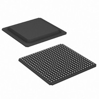
XC3S1600E-5FGG400C Xilinx Inc, XC3S1600E-5FGG400C Datasheet - Page 90

XC3S1600E-5FGG400C
Manufacturer Part Number
XC3S1600E-5FGG400C
Description
FPGA Spartan®-3E Family 1.6M Gates 33192 Cells 657MHz 90nm (CMOS) Technology 1.2V 400-Pin FBGA
Manufacturer
Xilinx Inc
Series
Spartan™-3Er
Datasheet
1.XC3S100E-4VQG100C.pdf
(233 pages)
Specifications of XC3S1600E-5FGG400C
Package
400FBGA
Family Name
Spartan®-3E
Device Logic Cells
33192
Device Logic Units
3688
Device System Gates
1600000
Number Of Registers
29504
Maximum Internal Frequency
657 MHz
Typical Operating Supply Voltage
1.2 V
Maximum Number Of User I/os
304
Ram Bits
663552
Number Of Logic Elements/cells
33192
Number Of Labs/clbs
3688
Total Ram Bits
663552
Number Of I /o
304
Number Of Gates
1600000
Voltage - Supply
1.14 V ~ 1.26 V
Mounting Type
Surface Mount
Operating Temperature
0°C ~ 85°C
Package / Case
400-BGA
Lead Free Status / RoHS Status
Lead free / RoHS Compliant
For Use With
HW-XA3S1600E-UNI-G - KIT DEVELOPMENT AUTOMOTIVE ECU
Lead Free Status / RoHS Status
Lead free / RoHS Compliant
Available stocks
Company
Part Number
Manufacturer
Quantity
Price
Company:
Part Number:
XC3S1600E-5FGG400C
Manufacturer:
XILINX
Quantity:
259
Company:
Part Number:
XC3S1600E-5FGG400C
Manufacturer:
Xilinx Inc
Quantity:
10 000
Part Number:
XC3S1600E-5FGG400C
Manufacturer:
XILINX/赛灵思
Quantity:
20 000
Functional Description
shows the minimum required number of address lines
between the FPGA and parallel Flash PROM. The actual
number of address line required depends on the density of
the attached parallel Flash PROM.
A multiple-FPGA daisy-chained application requires a paral-
lel Flash PROM large enough to contain the sum of the
FPGA file sizes. An application can also use a larger-density
Table 60: Number of Bits to Program a Spartan-3E FPGA and Smallest Parallel Flash PROM
Compatible Flash Families
The Spartan-3E BPI configuration interface operates with a
wide variety of x8 or x8/x16 parallel NOR Flash devices.
Table 61
with the Spartan-3E BPI interface. Consult the data sheet
for the desired parallel NOR Flash to determine its suitability
The basic timing requirements and waveforms are provided
in
(Module 3).
Table 61: Compatible Parallel NOR Flash Families
CCLK Frequency
In BPI mode, the FPGA’s internal oscillator generates the
configuration clock frequency that controls all the interface
timing. The FPGA starts configuration at its lowest fre-
quency and increases its frequency for the remainder of the
configuration process if so specified in the configuration bit-
stream. The maximum frequency is specified using the
ConfigRate
90
Numonyx
Atmel
Spansion
Macronix
Byte Peripheral Interface (BPI) Configuration Timing
Spartan-3E FPGA
XC3S1200E
XC3S1600E
XC3S100E
XC3S250E
XC3S500E
Flash Vendor
provides a few Flash memory families that operate
bitstream generator option.
Uncompressed
File Sizes (bits)
M29W, J3D StrataFlash
Flash Memory Family
1,353,728
2,270,208
3,841,184
5,969,696
581,344
AT29 / AT49
MX29
S29
www.xilinx.com
Parallel Flash PROM
parallel Flash PROM to hold additional data beyond just
FPGA configuration data. For example, the parallel Flash
PROM can also contain the application code for a MicroBlaze
RISC processor core implemented within the Spartan-3E
FPGA. After configuration, the MicroBlaze processor can
execute directly from external Flash or can copy the code to
other, faster system memory before executing the code.
Table 62: Maximum ConfigRate Settings for Parallel
Flash PROMs (Commercial Temperature Range)
Table 62
ous typical PROM read access times over the Commercial
temperature operating range. See
face (BPI) Configuration Timing
for more detailed information. Despite using slower
ConfigRate settings, BPI mode is equally fast as the other
configuration modes. In BPI mode, data is accessed at the
ConfigRate frequency and internally serialized with an 8X
clock frequency.
Using the BPI Interface after Configuration
After the FPGA successfully completes configuration, all
pins connected to the parallel Flash PROM are available as
user I/Os.
If not using the parallel Flash PROM after configuration,
drive LDC0 High to disable the PROM’s chip-select input.
The remainder of the BPI pins then become available to the
FPGA application, including all 24 address lines, the eight
data lines, and the LDC2, LDC1, and HDC control pins.
Because all the interface pins are user I/Os after configura-
tion, the FPGA application can continue to use the interface
pins to communicate with the parallel Flash PROM. Parallel
Flash PROMs are available in densities ranging from 1 Mbit
up to 128 Mbits and beyond. However, a single Spartan-3E
FPGA requires less than 6 Mbits for configuration. If
Smallest Usable
Flash Read Access Time
1 Mbit
2 Mbit
4 Mbit
4 Mbit
8 Mbit
shows the maximum ConfigRate settings for vari-
250 ns
115 ns
45 ns
DS312-2 (v3.8) August 26, 2009
Minimum Required
Maximum ConfigRate
Address Lines
(Module 3) and
Byte Peripheral Inter-
Product Specification
A[16:0]
A[17:0]
A[18:0]
A[18:0]
A[19:0]
Setting
12
3
6
UG332
R


