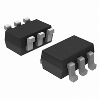
NSS12200WT1G ON Semiconductor, NSS12200WT1G Datasheet - Page 2

NSS12200WT1G
Manufacturer Part Number
NSS12200WT1G
Description
TRANSISTOR PNP 2A 12V SC-88
Manufacturer
ON Semiconductor
Datasheet
1.NSS12200WT1G.pdf
(5 pages)
Specifications of NSS12200WT1G
Transistor Type
PNP
Current - Collector (ic) (max)
2A
Voltage - Collector Emitter Breakdown (max)
12V
Vce Saturation (max) @ Ib, Ic
290mV @ 20mA, 1A
Current - Collector Cutoff (max)
100nA
Dc Current Gain (hfe) (min) @ Ic, Vce
100 @ 800mA, 1.5 V
Power - Max
450mW
Frequency - Transition
100MHz
Mounting Type
Surface Mount
Package / Case
SC-70-6, SC-88, SOT-363
Lead Free Status / RoHS Status
Lead free / RoHS Compliant
Other names
NSS12200WT1G
Available stocks
Company
Part Number
Manufacturer
Quantity
Price
Company:
Part Number:
NSS12200WT1G
Manufacturer:
ON Semiconductor
Quantity:
900
Company:
Part Number:
NSS12200WT1G
Manufacturer:
ON
Quantity:
30 000
1. FR−4, Minimum Pad, 1 oz Coverage.
2. FR−4, 1″ Pad, 1 oz Coverage.
3. Pulsed Condition: Pulse Width < 300 msec, Duty Cycle < 2%.
THERMAL CHARACTERISTICS
ELECTRICAL CHARACTERISTICS
OFF CHARACTERISTICS
ON CHARACTERISTICS
Total Device Dissipation
Thermal Resistance,
Total Device Dissipation
Thermal Resistance,
Thermal Resistance,
Total Device Dissipation
Junction and Storage
Collector −Emitter Breakdown Voltage, (I
Collector −Base Breakdown Voltage, (I
Emitter −Base Breakdown Voltage, (I
Collector Cutoff Current, (V
Collector−Emitter Cutoff Current, (V
Emitter Cutoff Current, (V
DC Current Gain (Note 3)
Collector −Emitter Saturation Voltage (Note 3)
Base −Emitter Saturation Voltage (Note 3)
Base −Emitter Turn−on Voltage (Note 3)
Cutoff Frequency
Output Capacitance
T
Derate above 25°C
Junction−to−Ambient
T
Derate above 25°C
Junction−to−Ambient
Junction−to−Lead 6
(Single Pulse < 10 sec.)
Temperature Range
(I
(I
(I
(I
(I
(I
(I
(I
(I
(V
A
A
C
C
C
C
C
C
C
C
C
CB
= 25°C
= 25°C
= −0.5 A, V
= −0.8 A, V
= −1.0 A, V
= −0.5 A, I
= −0.8 A, I
= −1.0 A, I
= −1.0 A, I
= −1.0 A, V
= −100 mA, V
= −1.5 V, f = 1.0 MHz)
B
B
B
B
CE
CE
CE
CE
= −10 mA)
= −16 mA)
= −20 mA)
= −20 mA)
CE
= −1.5 V)
= −1.5 V)
= −1.5 V)
= −1.5 V)
= −5.0 V, f = 100 MHz)
CES
CB
Characteristic
Characteristic
= −5.0 Vdc, I
= −12 Vdc, I
CES
E
C
= −0.1 mAdc, I
= −12 Vdc, I
C
= −0.1 mAdc, I
(T
= −10 mAdc, I
E
E
J
= 0)
= 0)
= 25°C unless otherwise noted)
E
C
= 0)
E
= 0)
B
http://onsemi.com
= 0)
= 0)
2
V
V
V
Symbol
V
V
V
(BR)CEO
(BR)CBO
(BR)EBO
CE(sat)
BE(sat)
C
I
I
I
BE(on)
R
R
CBO
h
CES
EBO
f
P
P
obo
FE
T
qJA
qJA
P
D
D
Symbol
T
D
(Note 1)
(Note 2)
R
J
(Note 1)
(Note 2)
Single
, T
qJL
stg
−5.0
Min
−12
−12
100
100
100
−
−
−
−
−
−
−
−
−
−
−55 to +150
−0.02
−0.03
−0.03
−0.10
−0.14
−0.17
−0.84
−0.81
−7.0
Typ
−15
−25
180
165
160
100
Max
50
450
275
650
192
105
3.6
5.2
1.4
−0.160
−0.235
−0.290
−0.95
−0.95
Max
−0.1
−0.1
−0.1
300
65
−
−
−
−
−
−
mW/°C
mW/°C
°C/W
°C/W
°C/W
Unit
mW
mW
°C
W
mAdc
mAdc
mAdc
MHz
Unit
Vdc
Vdc
Vdc
pF
V
V
V


