MJ21194G ON Semiconductor, MJ21194G Datasheet

TRANS PWR NPN 16A 250V TO3

MJ21194G

Manufacturer Part Number
MJ21194G
Description
TRANS PWR NPN 16A 250V TO3
Manufacturer
ON Semiconductor
Type
Powerr
Datasheets

Specifications of MJ21194G

Transistor Type
NPN
Current - Collector (ic) (max)
16A
Voltage - Collector Emitter Breakdown (max)
250V
Vce Saturation (max) @ Ib, Ic
4V @ 3.2A, 16A
Current - Collector Cutoff (max)
100µA
Dc Current Gain (hfe) (min) @ Ic, Vce
25 @ 8A, 5V
Power - Max
250W
Frequency - Transition
4MHz
Mounting Type
Chassis Mount
Package / Case
TO-204, TO-3
Transistor Polarity
NPN
Mounting Style
Through Hole
Collector- Emitter Voltage Vceo Max
250 V
Emitter- Base Voltage Vebo
5 V
Maximum Dc Collector Current
16 A
Power Dissipation
250 W
Maximum Operating Temperature
+ 200 C
Continuous Collector Current
16 A
Dc Collector/base Gain Hfe Min
25
Maximum Operating Frequency
4 MHz
Minimum Operating Temperature
- 65 C
Current, Collector
16 A
Current, Gain
8
Frequency
4 MHz
Package Type
TO-204AA (TO-3)
Polarity
NPN
Primary Type
Si
Resistance, Thermal, Junction To Case
0.7 °C/W
Voltage, Breakdown, Collector To Emitter
250 V
Voltage, Collector To Base
400 V
Voltage, Collector To Emitter
250 V
Voltage, Collector To Emitter, Saturation
4 V
Voltage, Emitter To Base
5 V
Lead Free Status / RoHS Status
Lead free / RoHS Compliant
Other names
MJ21194GOS

Available stocks

Company
Part Number
Manufacturer
Quantity
Price
Part Number:
MJ21194G
Manufacturer:
AD
Quantity:
501
MJ21193, MJ21194
Silicon Power Transistors
technology and are specifically designed for high power audio output,
disk head positioners and linear applications.
Features
Stresses exceeding Maximum Ratings may damage the device. Maximum
Ratings are stress ratings only. Functional operation above the Recommended
Operating Conditions is not implied. Extended exposure to stresses above the
Recommended Operating Conditions may affect device reliability.
1. Pulse Test: Pulse Width = 5 ms, Duty Cycle ≤ 10%. (continued)
*For additional information on our Pb−Free strategy and soldering details, please
© Semiconductor Components Industries, LLC, 2009
April, 2009 − Rev. 5
MAXIMUM RATINGS
THERMAL CHARACTERISTICS
download the ON Semiconductor Soldering and Mounting Techniques
Reference Manual, SOLDERRM/D.
Collector−Emitter Voltage
Collector−Base Voltage
Emitter−Base Voltage
Collector−Emitter Voltage − 1.5 V
Collector Current − Continuous
Base Current − Continuous
Total Power Dissipation @ T
Derate Above 25°C
Operating and Storage Junction
Temperature Range
Thermal Resistance, Junction−to−Case
The MJ21193 (PNP) and MJ21194 (NPN) utilize Perforated Emitter
Total Harmonic Distortion Characterized
High DC Current Gain − h
Excellent Gain Linearity
High SOA: 2.5 A, 80 V, 1 Second
Pb−Free Packages are Available*
Characteristic
Rating
Peak (Note 1)
C
Preferred Device
= 25°C
FE
= 25 Min @ I
Symbol
Symbol
T
V
V
V
V
R
J
P
, T
CEO
CBO
EBO
CEX
I
I
qJC
C
B
D
stg
C
= 8 Adc
− 65 to +200
Value
1.43
Max
250
400
400
250
0.7
16
30
5
5
1
W/°C
°C/W
Unit
Unit
Vdc
Vdc
Vdc
Vdc
Adc
Adc
°C
W
Preferred devices are recommended choices for future use
and best overall value.
†For information on tape and reel specifications,
MJ21193
MJ21193G
MJ21194
MJ21194G
including part orientation and tape sizes, please
refer to our Tape and Reel Packaging Specifications
Brochure, BRD8011/D.
16 AMP COMPLEMENTARY
Device
TO−204AA (TO−3)
250 VOLTS, 250 WATTS
CASE 1−07
STYLE 1
ORDERING INFORMATION
MJ2119x = Device Code
G
A
YY
WW
MEX
SILICON POWER
TRANSISTORS
http://onsemi.com
(Pb−Free)
(Pb−Free)
Package
TO−3
TO−3
TO−3
TO−3
= Pb−Free Package
= Assembly Location
= Year
= Work Week
= Country of Origin
x = 3 or 4
Publication Order Number:
100 Units / Tray
100 Units / Tray
100 Units / Tray
100 Units / Tray
Shipping
MJ2119xG
MARKING
DIAGRAM
AYYWW
MEX
MJ21193/D

Related parts for MJ21194G

MJ21194G Summary of contents

Page 1

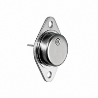
... Units / Tray MJ21193G TO−3 100 Units / Tray (Pb−Free) MJ21194 TO−3 100 Units / Tray MJ21194G TO−3 100 Units / Tray (Pb−Free) †For information on tape and reel specifications, including part orientation and tape sizes, please refer to our Tape and Reel Packaging Specifications Brochure, BRD8011/D. ...

Page 2

ELECTRICAL CHARACTERISTICS Characteristic OFF CHARACTERISTICS Collector−Emitter Sustaining Voltage (I = 100 mAdc Collector Cutoff Current (V = 200 Vdc Emitter Cutoff Current ( Vdc ...

Page 3

PNP MJ21193 1000 T = 100°C J 25°C 100 0.1 1.0 I COLLECTOR CURRENT (AMPS) C Figure 3. DC Current Gain, V PNP MJ21193 1000 T = 100°C J 25°C 100 - 25°C V ...

Page 4

PNP MJ21193 3.0 2 25° 2 1.5 1.0 V BE(sat) 0.5 V CE(sat) 0 0.1 1 COLLECTOR CURRENT (AMPS) C Figure 9. Typical Saturation Voltages PNP MJ21193 10 ...

Page 5

25° 1000 MHz (test) 100 0.1 1 REVERSE VOLTAGE (VOLTS) R Figure 14. MJ21193 Typical Capacitance 1.2 1.1 1.0 0.9 0.8 0.7 0.6 10 AUDIO PRECISION MODEL ...

Page 6

... Opportunity/Affirmative Action Employer. This literature is subject to all applicable copyright laws and is not for resale in any manner. PUBLICATION ORDERING INFORMATION LITERATURE FULFILLMENT: Literature Distribution Center for ON Semiconductor P.O. Box 5163, Denver, Colorado 80217 USA Phone: 303−675−2175 or 800−344−3860 Toll Free USA/Canada Fax: 303− ...

Related keywords