MJ21194G ON Semiconductor, MJ21194G Datasheet - Page 2
MJ21194G
Manufacturer Part Number
MJ21194G
Description
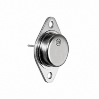
TRANS PWR NPN 16A 250V TO3
Manufacturer
ON Semiconductor
Type
Powerr
Specifications of MJ21194G
Transistor Type
NPN
Current - Collector (ic) (max)
16A
Voltage - Collector Emitter Breakdown (max)
250V
Vce Saturation (max) @ Ib, Ic
4V @ 3.2A, 16A
Current - Collector Cutoff (max)
100µA
Dc Current Gain (hfe) (min) @ Ic, Vce
25 @ 8A, 5V
Power - Max
250W
Frequency - Transition
4MHz
Mounting Type
Chassis Mount
Package / Case
TO-204, TO-3
Transistor Polarity
NPN
Mounting Style
Through Hole
Collector- Emitter Voltage Vceo Max
250 V
Emitter- Base Voltage Vebo
5 V
Maximum Dc Collector Current
16 A
Power Dissipation
250 W
Maximum Operating Temperature
+ 200 C
Continuous Collector Current
16 A
Dc Collector/base Gain Hfe Min
25
Maximum Operating Frequency
4 MHz
Minimum Operating Temperature
- 65 C
Current, Collector
16 A
Current, Gain
8
Frequency
4 MHz
Package Type
TO-204AA (TO-3)
Polarity
NPN
Primary Type
Si
Resistance, Thermal, Junction To Case
0.7 °C/W
Voltage, Breakdown, Collector To Emitter
250 V
Voltage, Collector To Base
400 V
Voltage, Collector To Emitter
250 V
Voltage, Collector To Emitter, Saturation
4 V
Voltage, Emitter To Base
5 V
Lead Free Status / RoHS Status
Lead free / RoHS Compliant
Other names
MJ21194GOS
Available stocks
Company
Part Number
Manufacturer
Quantity
Price


NOTE:
ELECTRICAL CHARACTERISTICS
OFF CHARACTERISTICS
SECOND BREAKDOWN
ON CHARACTERISTICS
DYNAMIC CHARACTERISTICS
Collector−Emitter Sustaining Voltage
Collector Cutoff Current
Emitter Cutoff Current
Collector Cutoff Current
Second Breakdown Collector Current with Base Forward Biased
DC Current Gain
Base−Emitter On Voltage
Collector−Emitter Saturation Voltage
Total Harmonic Distortion at the Output
Current Gain Bandwidth Product
Output Capacitance
6.5
6.0
5.5
5.0
4.5
4.0
3.5
3.0
(I
(V
(V
(V
(V
(V
(I
(I
(I
(I
(I
V
(Matched pair h
(I
(V
0.1
C
C
C
C
C
C
C
RMS
CE
CE
CE
CE
CE
CB
= 100 mAdc, I
= 8 Adc, V
= 16 Adc, I
= 8 Adc, V
= 8 Adc, I
= 16 Adc, I
= 1 Adc, V
T
f
5 V
test
V
J
Pulse Test: Pulse Width = 300 ms, Duty Cycle ≤2%
= 200 Vdc, I
= 5 Vdc, I
= 250 Vdc, V
= 50 Vdc, t = 1 s (non−repetitive)
= 80 Vdc, t = 1 s (non−repetitive)
= 10 Vdc, I
CE
= 25°C
= 28.3 V, f = 1 kHz, P
= 1 MHz
= 10 V
Figure 1. Typical Current Gain
B
CE
CE
CE
B
B
= 0.8 Adc)
C
I
FE
C
= 5 Adc)
= 3.2 Adc)
E
= 0)
= 5 Vdc)
= 5 Vdc)
= 10 Vdc, f
B
B
COLLECTOR CURRENT (AMPS)
= 0, f
BE(off)
= 50 @ 5 A/5 V)
Bandwidth Product
= 0)
= 0)
PNP MJ21193
test
= 1.5 Vdc)
Characteristic
= 1 MHz)
LOAD
test
1.0
= 1 MHz)
= 100 W
(T
C
RMS
= 25°C unless otherwise noted)
h
unmatched
h
matched
FE
FE
http://onsemi.com
10
2
7.0
5.0
4.0
3.0
2.0
1.0
8.0
6.0
0
0.1
V
Symbol
V
V
CEO(sus)
CE(sat)
T
f
I
I
I
BE(on)
T
C
test
CEO
I
h
EBO
CEX
J
S/b
f
FE
HD
T
ob
= 25°C
= 1 MHz
Figure 2. Typical Current Gain
I
C
COLLECTOR CURRENT (AMPS)
Bandwidth Product
NPN MJ21194
Min
250
2.5
25
−
−
−
5
8
−
−
−
−
−
4
−
1.0
0.08
Typ
0.8
−
−
−
−
−
−
−
−
−
−
−
−
V
CE
Max
100
100
100
500
2.2
1.4
75
−
−
−
4
−
−
−
= 5 V
10 V
mAdc
mAdc
mAdc
MHz
Unit
Vdc
Adc
Vdc
Vdc
pF
%
10
Related parts for MJ21194G
Image
Part Number
Description
Manufacturer
Datasheet
Request
R

Part Number:
Description:
ON Semiconductor [VOLTAGE REGULATOR]
Manufacturer:
ON Semiconductor
Datasheet:
Part Number:
Description:
357-036-542-201 CARDEDGE 36POS DL .156 BLK LOPRO
Manufacturer:
ON Semiconductor
Datasheet:
Part Number:
Description:
357-036-542-201 CARDEDGE 36POS DL .156 BLK LOPRO
Manufacturer:
ON Semiconductor
Datasheet:
Part Number:
Description:
357-036-542-201 CARDEDGE 36POS DL .156 BLK LOPRO
Manufacturer:
ON Semiconductor
Datasheet:
Part Number:
Description:
357-036-542-201 CARDEDGE 36POS DL .156 BLK LOPRO
Manufacturer:
ON Semiconductor
Datasheet:
Part Number:
Description:
357-036-542-201 CARDEDGE 36POS DL .156 BLK LOPRO
Manufacturer:
ON Semiconductor
Datasheet:
Part Number:
Description:
357-036-542-201 CARDEDGE 36POS DL .156 BLK LOPRO
Manufacturer:
ON Semiconductor
Datasheet:
Part Number:
Description:
357-036-542-201 CARDEDGE 36POS DL .156 BLK LOPRO
Manufacturer:
ON Semiconductor
Datasheet:
Part Number:
Description:
357-036-542-201 CARDEDGE 36POS DL .156 BLK LOPRO
Manufacturer:
ON Semiconductor
Datasheet:
Part Number:
Description:
357-036-542-201 CARDEDGE 36POS DL .156 BLK LOPRO
Manufacturer:
ON Semiconductor
Datasheet:
Part Number:
Description:
357-036-542-201 CARDEDGE 36POS DL .156 BLK LOPRO
Manufacturer:
ON Semiconductor
Datasheet:
Part Number:
Description:
Manufacturer:
ON Semiconductor
Datasheet:
Part Number:
Description:
Manufacturer:
ON Semiconductor
Datasheet:
Part Number:
Description:
Manufacturer:
ON Semiconductor
Datasheet: