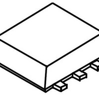
NJG1107KB2-TE1 NJR, NJG1107KB2-TE1 Datasheet - Page 4

NJG1107KB2-TE1
Manufacturer Part Number
NJG1107KB2-TE1
Description
RF Amplifier 1.5/1.9 GHz LwNoise
Manufacturer
NJR
Type
General Purpose Amplifierr
Datasheet
1.NJG1107KB2-TE1.pdf
(19 pages)
Specifications of NJG1107KB2-TE1
Operating Frequency
1.5 GHz to 1.9 GHz
P1db
- 2 dBm
Noise Figure
1.2 dB
Supply Current
3.8 mA
Maximum Power Dissipation
450 mW
Maximum Operating Temperature
+ 85 C
Mounting Style
SMD/SMT
Package / Case
FLP-6-B2
Minimum Operating Temperature
- 40 C
Number Of Channels
1 Channel
Lead Free Status / RoHS Status
Lead free / RoHS Compliant
Available stocks
Company
Part Number
Manufacturer
Quantity
Price
Company:
Part Number:
NJG1107KB2-TE1
Manufacturer:
JRC
Quantity:
12 000
NJG1107KB2
nPIN CONFIGURATION
2,4,5 GND
- 4 -
Pin
1
3
6
RFout
EXTCAP
RFin
Function
RF output and voltage supply pin. External matching circuits and a bypass capacitor
is required. L3 is a RF choke inductor and C1 is a DC blocking capacitor. These
elements are used as output matching circuit. C2 is a bypass capacitor. (Please refer
to “TEST CIRCUIT”)
Ground pin. To keep good RF grounding performance, please use multiple via holes
to connect with ground plane and this pin.
An external bypass capacitor is required. (Please refer to “TEST CIRCUIT”)
RF input pin. A DC blocking capacitor is not required. An external matching circuit is
required. (Please refer to “TEST CIRCUIT”)
Description


