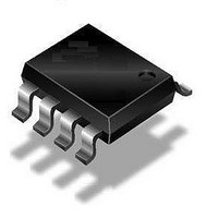
ATA6620N-TASY Atmel, ATA6620N-TASY Datasheet - Page 11

ATA6620N-TASY
Manufacturer Part Number
ATA6620N-TASY
Description
RF Wireless Misc LIN SBC
Manufacturer
Atmel
Datasheet
1.ATA6620N-TAQY.pdf
(22 pages)
Specifications of ATA6620N-TASY
Package / Case
SOIC
Mounting Style
SMD/SMT
Lead Free Status / RoHS Status
Lead free / RoHS Compliant
4.4
5. Fail-safe Features
4850I–AUTO–09/09
Unpowered Mode
If battery voltage is connected to the application circuit (see
pin increases due to the block capacitor. When V
V
reaches nominal value after t
NRES is low for the reset time delay t
Figure 4-7.
Sth
• During a short circuit at LIN, the output limits the output current to I
• There are now reverse currents < 3 µA at pin LIN during loss of V
• During a short circuit at VCC, the output limits the output current to I
• Pin EN provides a pull-down resistor to force the transceiver into recessive mode if EN is
• Pin RXD is set floating if V
• Pin TXD provides a pull-up resistor to force the transceiver into recessive mode if TXD is
dissipation, the chip temperature exceeds t
cools down and after a hysteresis of t
overtemperature switch-off, the V
behavior for bus systems where some slave nodes are supplied from battery or ignition.
undervoltage, NRES switches to low and sends a reset to the microcontroller. The IC
switches into Pre–normal mode. If the chip temperature exceeds the value t
output switches off. The chip cools down and after a hysteresis of t
again. Because of Pre-normal mode, the V
switched off from the microcontroller.The microcontroller can then start with normal
operation.
disconnected.
disconnected.
, the IC-mode changes from Unpowered to Pre-normal mode. The V
NRES
VCC
VS
5.5V
V
12V
V
3V
thun
5V
5V
CC
Voltage Regulator: Ramp Up and Undervoltage
t
VCC
VCC
Batt
. This time depends on the V
is disconnected.
CC
Reset
t
res
regulator works independently.
hys
; no mode change is possible during this time.
, switches the output on again. During LIN
CC
LINoff
voltage will switch on again although EN is
S
is higher than the V
and the LIN output is switched off. The chip
CC
Figure
capacitor and the load.
Batt
4-7), the voltage at the VS
t
hys
es_f
BUS_LIM
S
VCCn
, switches the output on
or GND. This is optimal
undervoltage threshold,
. Because of
ATA6620N
. Due to the power
CC
VCCoff
output voltage
, the V
CC
11


