MAX9627ETC+ Maxim Integrated Products, MAX9627ETC+ Datasheet
MAX9627ETC+
Specifications of MAX9627ETC+


Related parts for MAX9627ETC+

MAX9627ETC+ Summary of contents
Page 1
... Applications Communication Medical Imaging ATE High-Performance Instrumentation SINGLE-ENDED INPUT _______________________________________________________________ Maxim Integrated Products 1 For pricing, delivery, and ordering information, please contact Maxim Direct at 1-888-629-4642, or visit Maxim’s website at www.maxim-ic.com. Low-Noise, Low-Distortion, Low-Voltage Noise Density 3.6nV/√Hz S Low Harmonic Distortion S ...
Page 2
Low-Noise, Low-Distortion, 1.35GHz Fully Differential Amplifiers ABSOLUTE MAXIMUM RATINGS Supply Voltage ( )................................-0.3V to +5. IN+, IN- ...........................................(V EE RT+, RT- .........................................(V EE RT- to IN- and RT+ to IN+ .................................................... Q2V VOCM, SHDN, OUT+, OUT- ...
Page 3
Fully Differential Amplifiers ELECTRICAL CHARACTERISTICS (continued +3.3V 0V 0V, SHDN = IN- IN+ +125°C. Typical values are at +25°C, unless otherwise noted.) (Note 1) PARAMETER SYMBOL Common-Mode Rejection ...
Page 4
Low-Noise, Low-Distortion, 1.35GHz Fully Differential Amplifiers ELECTRICAL CHARACTERISTICS (continued +3.3V 0V 0V, SHDN = IN- IN+ +125°C. Typical values are at +25°C, unless otherwise noted.) (Note 1) PARAMETER SYMBOL ...
Page 5
Fully Differential Amplifiers (V = +3.3V 0V 0V, SHDN = IN- IN+ versions, unless noted otherwise.) HARMONIC DISTORTION vs. FREQUENCY R = 100I -40 MAX9626 ...
Page 6
Low-Noise, Low-Distortion, 1.35GHz Fully Differential Amplifiers (V = +3.3V 0V 0V, SHDN = IN- IN+ versions, unless noted otherwise.) HARMONIC DISTORTION vs. LOAD f = 10MHz -60 ...
Page 7
Fully Differential Amplifiers (V = +3.3V 0V 0V, SHDN = IN- IN+ versions, unless noted otherwise.) HARMONIC DISTORTION vs. DIFFERENTIAL OUTPUT SWING f = 125MHz -60 ...
Page 8
Low-Noise, Low-Distortion, 1.35GHz Fully Differential Amplifiers (V = +3.3V 0V 0V, SHDN = IN- IN+ versions, unless noted otherwise.) LARGE-SIGNAL BANDWIDTH vs. FREQUENCY V = 3.3V 100I ...
Page 9
Fully Differential Amplifiers (V = +3.3V 0V 0V, SHDN = IN- IN+ versions, unless noted otherwise.) SMALL-SIGNAL BANDWIDTH vs. V VOCM 1 ...
Page 10
Low-Noise, Low-Distortion, 1.35GHz Fully Differential Amplifiers (V = +3.3V 0V 0V, SHDN = IN- IN+ versions, unless noted otherwise.) POWER-SUPPLY REJECTION RATIO vs. FREQUENCY (MAX9626) 100 ...
Page 11
Fully Differential Amplifiers (V = +3.3V 0V 0V, SHDN = IN- IN+ versions, unless noted otherwise.) SUPPLY CURRENT vs. SUPPLY VOLTAGE 64 MAX9627 MAX9628 MAX9626 ...
Page 12
Low-Noise, Low-Distortion, 1.35GHz Fully Differential Amplifiers (V = +3.3V 0V 0V, SHDN = IN- IN+ versions, unless noted otherwise.) INTERMODULATION DISTORTION vs. FREQUENCY (MAX9628 5V) CC -50 FREQUENCY SPACING ...
Page 13
Fully Differential Amplifiers (V = +3.3V 0V 0V, SHDN = IN- IN+ versions, unless noted otherwise.)versions, unless noted otherwise.) VOCM TRANSIENT RESPONSE (MAX9628 1.6V TO 1.7V STEP) IN ...
Page 14
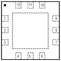
Low-Noise, Low-Distortion, 1.35GHz Fully Differential Amplifiers TOP VIEW PIN NAME 1 IN+ Noninverting Differential Input 2 VOCM Output Common-Mode Voltage Input 3 IN- Inverting Differential Input 4 RT- Termination Resistor Terminal for IN Positive Supply Voltage CC ...
Page 15
Fully Differential Amplifiers Detailed Description The MAX9626/MAX9627/MAX9628 family employs voltage feedback to implement a differential-in to differential-out amplifier. On-chip feedback resistors set the gain of the amplifier. The use of on-chip resistors not only saves cost and space, but ...
Page 16
Low-Noise, Low-Distortion, 1.35GHz Fully Differential Amplifiers Table 2. Typical Gain Values When Using the Internal Termination Resistors (R and ( 200 200 64 150 300 64 125 ...
Page 17
Fully Differential Amplifiers Input Voltage Noise The input referred voltage noise specification reported in the Electrical Characteristics table includes both the noise contribution of the amplifier and the contribution of all the internal resistive elements. Because such resistive elements ...
Page 18
Low-Noise, Low-Distortion, 1.35GHz Fully Differential Amplifiers For the latest package outline information and land patterns (footprints www.maxim-ic.com/packages. Note that a “+”, “#”, or “-” in the package code indicates RoHS status only. Package drawings may show a different ...
Page 19
Fully Differential Amplifiers For the latest package outline information and land patterns (footprints www.maxim-ic.com/packages. Note that a “+”, “#”, or “-” in the package code indicates RoHS status only. Package drawings may show a different suffix character, ...
Page 20
... Maxim cannot assume responsibility for use of any circuitry other than circuitry entirely embodied in a Maxim product. No circuit patent licenses are implied. Maxim reserves the right to change the circuitry and specifications without notice at any time. Maxim Integrated Products, 120 San Gabriel Drive, Sunnyvale, CA 94086 408-737-7600 20 2011 Maxim Integrated Products © ...