MAX9627ETC+ Maxim Integrated Products, MAX9627ETC+ Datasheet - Page 15
MAX9627ETC+
Manufacturer Part Number
MAX9627ETC+
Description
RF Amplifier LW NOISE/DISTORTION DIFFERENTIAL AMP
Manufacturer
Maxim Integrated Products
Datasheet
1.MAX9627ETC.pdf
(20 pages)
Specifications of MAX9627ETC+
Bandwidth
1350 MHz
Operating Supply Voltage
2.85 V to 5.25 V
Supply Current
59 mA
Maximum Power Dissipation
1333 mW
Maximum Operating Temperature
+ 125 C
Mounting Style
SMD/SMT
Package / Case
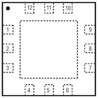
TQFN-12
Minimum Operating Temperature
- 40 C
Lead Free Status / RoHS Status
Lead free / RoHS Compliant


The MAX9626/MAX9627/MAX9628 family employs
voltage feedback to implement a differential-in to
differential-out amplifier. On-chip feedback resistors set
the gain of the amplifier. The use of on-chip resistors
not only saves cost and space, but also maximizes the
overall amplifier’s performance.
There are two feedback loops within the amplifier
circuit. The differential feedback loop employs the on-
chip resistors to set the differential gain. The signal is
applied differentially at the inputs and the output signal is
obtained differentially at the outputs. The common-mode
feedback loop controls the common-mode voltage at the
outputs. Both inverting and noninverting outputs exhibit
a common-mode voltage equal to the voltage applied
at VOCM input, without affecting the differential output
signal. The outputs are perfectly balanced having
signals of equal amplitude and 180N apart in-phase.
Amplifier input impedance is determined by internal
gain resistors. Therefore, source impedance does affect
the gain of the amplifier. Input termination resistors
are required to achieve source impedance match. If
preferred, the customer has the choice of using the
on-chip termination resistors. If they are used, then
the amplifier’s input impedance is 50I for single-
ended input configuration. The amplifier’s differential gain
accuracy is directly affected by the source impedance
value.
The ICs feature a proprietary circuit design. The use
of predistortion and dynamic distortion cancellation
greatly improves large-signal AC-performance at high
frequency.
The ICs have internal gain resistors to achieve
excellent bandwidth and distortion performance. Because
the virtual ground nodes among the gain resistors and
the inputs of the amplifier are internal to the device, the
parasitic capacitors of such nodes are kept to the
minimum. This enhances the AC performance of the
device.
Detailed Description
Fixed Gain Options for
1.35GHz Fully Differential Amplifiers
Best AC Performance
Low-Noise, Low-Distortion,
The ICs have three gain options with resistor values as
per Table 1, while keeping the bandwidth constant.
Table 1. Amplifier’s Gain Setting and
Internal Resistor Values
The differential gain is given by the equation: G = R
Use the internal R
source impedance R
of the amplifier has to match with it. For a perfectly
balanced circuit driven by a differential source
impedance, the input impedance of the amplifier is given
by the simple equation R
input applications, where the source impedance of 50I
connects to either input, such as in the Typical Operating
Circuit, the input impedance of the amplifier is given by
the equation:
To match the input impedance R
tion must be met: R
Therefore:
From this equation it can be inferred that R
for all the cases of Table 1.
GAIN (V/V)
1
2
4
R
T
=
R
R
IN
1
G
200
150
125
−
T
(I)
=
IN
0.5 x
resistors in applications where the
S
||R
1
is 50I and the input impedance
−
T
2 x (R
IN
= R
R
R
R
S
G
= 2 x R
Internal Terminations
R
R
G
R
S
S
G
R
(
F
200
300
500
G
R
+
F
(I)
F
R
+
S
F
+
R )
, the following condi-
2 x R
G
F
. For single-ended
G
BANDWIDTH
T
)
is about 64I
(GHz)
1.35
1.15
3dB
1
F
/R
15
G
Related parts for MAX9627ETC+
Image
Part Number
Description
Manufacturer
Datasheet
Request
R

Part Number:
Description:
MAX7528KCWPMaxim Integrated Products [CMOS Dual 8-Bit Buffered Multiplying DACs]
Manufacturer:
Maxim Integrated Products
Datasheet:
Part Number:
Description:
Single +5V, fully integrated, 1.25Gbps laser diode driver.
Manufacturer:
Maxim Integrated Products
Datasheet:
Part Number:
Description:
Single +5V, fully integrated, 155Mbps laser diode driver.
Manufacturer:
Maxim Integrated Products
Datasheet:
Part Number:
Description:
VRD11/VRD10, K8 Rev F 2/3/4-Phase PWM Controllers with Integrated Dual MOSFET Drivers
Manufacturer:
Maxim Integrated Products
Datasheet:
Part Number:
Description:
Highly Integrated Level 2 SMBus Battery Chargers
Manufacturer:
Maxim Integrated Products
Datasheet:
Part Number:
Description:
Current Monitor and Accumulator with Integrated Sense Resistor; ; Temperature Range: -40°C to +85°C
Manufacturer:
Maxim Integrated Products
Part Number:
Description:
TSSOP 14/A�/RS-485 Transceivers with Integrated 100O/120O Termination Resis
Manufacturer:
Maxim Integrated Products
Part Number:
Description:
TSSOP 14/A�/RS-485 Transceivers with Integrated 100O/120O Termination Resis
Manufacturer:
Maxim Integrated Products
Part Number:
Description:
QFN 16/A�/AC-DC and DC-DC Peak-Current-Mode Converters with Integrated Step
Manufacturer:
Maxim Integrated Products
Part Number:
Description:
TDFN/A/65V, 1A, 600KHZ, SYNCHRONOUS STEP-DOWN REGULATOR WITH INTEGRATED SWI
Manufacturer:
Maxim Integrated Products
Part Number:
Description:
Integrated Temperature Controller f
Manufacturer:
Maxim Integrated Products
Part Number:
Description:
SOT23-6/I�/45MHz to 650MHz, Integrated IF VCOs with Differential Output
Manufacturer:
Maxim Integrated Products
Part Number:
Description:
SOT23-6/I�/45MHz to 650MHz, Integrated IF VCOs with Differential Output
Manufacturer:
Maxim Integrated Products
Part Number:
Description:
EVALUATION KIT/2.4GHZ TO 2.5GHZ 802.11G/B RF TRANSCEIVER WITH INTEGRATED PA
Manufacturer:
Maxim Integrated Products
Part Number:
Description:
QFN/E/DUAL PCIE/SATA HIGH SPEED SWITCH WITH INTEGRATED BIAS RESISTOR
Manufacturer:
Maxim Integrated Products
Datasheet: