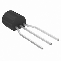
MPS751ZL1G ON Semiconductor, MPS751ZL1G Datasheet - Page 2

MPS751ZL1G
Manufacturer Part Number
MPS751ZL1G
Description
TRANSISTOR PNP GP 2A 60V TO-92
Manufacturer
ON Semiconductor
Datasheet
1.MPS751RLRAG.pdf
(5 pages)
Specifications of MPS751ZL1G
Transistor Type
PNP
Current - Collector (ic) (max)
2A
Voltage - Collector Emitter Breakdown (max)
60V
Vce Saturation (max) @ Ib, Ic
500mV @ 200mA, 2A
Dc Current Gain (hfe) (min) @ Ic, Vce
75 @ 1A, 2V
Power - Max
625mW
Frequency - Transition
75MHz
Mounting Type
Through Hole
Package / Case
TO-92-3 (Standard Body), TO-226
Lead Free Status / RoHS Status
Lead free / RoHS Compliant
Current - Collector Cutoff (max)
-
ELECTRICAL CHARACTERISTICS
OFF CHARACTERISTICS
ON CHARACTERISTICS (Note 1)
SMALL−SIGNAL CHARACTERISTICS
1. Pulse Test: Pulse Width ≤ 300 ms, Duty Cycle = 2.0%.
2. f
Collector −Emitter Breakdown Voltage (Note 1)
Collector −Base Breakdown Voltage
Emitter −Base Breakdown Voltage
Collector Cutoff Current
Emitter Cutoff Current
DC Current Gain
Collector −Emitter Saturation Voltage
Base−Emitter On Voltage
Base −Emitter Saturation Voltage
Current −Gain − Bandwidth Product (Note 2)
300
270
240
210
180
150
120
90
60
30
T
0
(I
(I
(I
(V
(V
(V
(I
(I
(I
(I
(I
(I
(I
(I
(I
10
is defined as the frequency at which |h
C
C
C
C
C
C
C
C
C
C
C
C
CB
CB
EB
= 10 mAdc, I
= 100 mAdc, I
= 0, I
= 50 mA, V
= 500 mA, V
= 1.0 A, V
= 2.0 A, V
= 2.0 A, I
= 1.0 A, I
= 1.0 A, V
= 1.0 A, I
= 50 mAdc, V
T
J
−55 °C
= 4.0 V, I
= 60 Vdc, I
= 80 Vdc, I
20
= 125°C
25°C
E
= 10 mAdc)
B
B
B
CE
CE
CE
50
Figure 1. MPS650, MPS651
C
= 200 mA)
= 100 mA)
= 100 mA)
CE
Typical DC Current Gain
CE
B
I
E
E
= 0)
= 2.0 V)
= 2.0 V)
= 2.0 V)
E
C
CE
, COLLECTOR CURRENT (mA)
= 2.0 V)
= 0)
= 0)
= 0)
= 0 )
= 2.0 V)
100
= 5.0 Vdc, f = 100 MHz)
NPN − MPS650, MPS651; PNP − MPS750, MPS751
200
NPN
Characteristic
500 1.0 A 2.0 A 4.0 A
(T
C
fe
| extrapolates to unity.
= 25°C unless otherwise noted)
V
CE
= 2.0 V
http://onsemi.com
MPS650, MPS750
MPS651, MPS751
MPS650, MPS750
MPS651, MPS751
MPS650, MPS750
MPS651, MPS751
2
250
225
200
175
150
125
100
75
50
25
0
−10 −20
T
J
= 125°C
25°C
−55 °C
−50 −100 −200
V
V
Figure 2. MPS750, MPS751
V
Symbol
V
V
V
(BR)CEO
(BR)CBO
Typical DC Current Gain
(BR)EBO
I
I
I
CE(sat)
BE(sat)
BE(on)
C
h
CBO
EBO
, COLLECTOR CURRENT (mA)
f
FE
T
PNP
Min
5.0
40
60
60
80
75
75
75
40
75
−
−
−
−
−
−
−
−500
−1.0 A −2.0 A −4.0 A
Max
0.1
0.1
0.1
0.5
0.3
1.0
1.2
−
−
−
−
−
−
−
−
−
−
V
CE
= −2.0 V
mAdc
mAdc
MHz
Unit
Vdc
Vdc
Vdc
Vdc
Vdc
Vdc
−


