MJD42C1G ON Semiconductor, MJD42C1G Datasheet

TRANS POWER PNP 6A 100V DPAK

MJD42C1G

Manufacturer Part Number
MJD42C1G
Description
TRANS POWER PNP 6A 100V DPAK
Manufacturer
ON Semiconductor
Datasheet

Specifications of MJD42C1G

Transistor Type
PNP
Current - Collector (ic) (max)
6A
Voltage - Collector Emitter Breakdown (max)
100V
Vce Saturation (max) @ Ib, Ic
1.5V @ 600mA, 6A
Current - Collector Cutoff (max)
50µA
Dc Current Gain (hfe) (min) @ Ic, Vce
15 @ 3A, 4V
Power - Max
1.75W
Frequency - Transition
3MHz
Mounting Type
Through Hole
Package / Case
IPak, TO-251, DPak, VPak (3 straight leads + tab)
Configuration
Single
Transistor Polarity
PNP
Mounting Style
SMD/SMT
Collector- Emitter Voltage Vceo Max
100 V
Emitter- Base Voltage Vebo
5 V
Continuous Collector Current
6 A
Maximum Dc Collector Current
6 A
Power Dissipation
20 W
Maximum Operating Frequency
3 MHz
Maximum Operating Temperature
+ 150 C
Dc Collector/base Gain Hfe Min
30 at 0.3 A at 4 V
Minimum Operating Temperature
- 65 C
Lead Free Status / RoHS Status
Lead free / RoHS Compliant

Available stocks

Company
Part Number
Manufacturer
Quantity
Price
Part Number:
MJD42C1G
Manufacturer:
ON
Quantity:
12 500
MJD41C (NPN)
MJD42C (PNP)
Complementary Power
Transistors
DPAK For Surface Mount Applications
applications.
Features
Stresses exceeding Maximum Ratings may damage the device. Maximum
Ratings are stress ratings only. Functional operation above the Recommended
Operating Conditions is not implied. Extended exposure to stresses above the
Recommended Operating Conditions may affect device reliability.
1. These ratings are applicable when surface mounted on the minimum pad
© Semiconductor Components Industries, LLC, 2011
January, 2011 − Rev. 9
MAXIMUM RATINGS
THERMAL CHARACTERISTICS
Collector−Emitter Voltage
Collector−Base Voltage
Emitter−Base Voltage
Collector Current
Base Current
Total Power Dissipation @ T
Total Power Dissipation (Note 1)
Operating and Storage Junction
Thermal Resistance, Junction−to−Case
Thermal Resistance, Junction−to−Ambient
(Note 1)
Designed for general purpose amplifier and low speed switching
(No Suffix)
Lead Formed for Surface Mount Applications in Plastic Sleeves
Straight Lead Version in Plastic Sleeves (“1” Suffix)
Electrically Similar to Popular TIP41 and TIP42 Series
Epoxy Meets UL 94 V−0 @ 0.125 in
ESD Ratings: Human Body Model, 3B u 8000 V
These are Pb−Free Packages
sizes recommended.
Derate above 25°C
@ T
Derate above 25°C
Temperature Range
A
= 25°C
Characteristic
Rating
Machine Model, C u 400 V
− Continuous
− Peak
C
= 25°C
Symbol
Symbol
T
V
R
R
J
V
V
P
P
CEO
, T
I
I
qJC
qJA
CB
EB
C
B
D
D
stg
−65 to +150
0.014
Max
0.16
1.75
Max
6.25
71.4
100
100
10
20
5
6
2
1
W/°C
W/°C
°C/W
°C/W
Unit
Unit
Vdc
Vdc
Vdc
Adc
Adc
°C
W
W
See detailed ordering and shipping information in the package
dimensions section on page 2 of this data sheet.
1 2
1
POWER TRANSISTORS
2
100 VOLTS, 20 WATTS
3
ORDERING INFORMATION
3
A
Y
WW
J4xC = Device Code
G
http://onsemi.com
4
6 AMPERES
4
= Assembly Location
= Year
= Work Week
= Pb−Free Package
SILICON
CASE 369C
CASE 369D
x = 1 or 2
STYLE 1
STYLE 1
DPAK−3
DPAK
Publication Order Number:
DIAGRAMS
MARKING
AYWW
J4xCG
AYWW
J4xCG
MJD41C/D

Related parts for MJD42C1G

MJD42C1G Summary of contents

Page 1

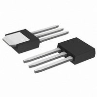
MJD41C (NPN) MJD42C (PNP) Complementary Power Transistors DPAK For Surface Mount Applications Designed for general purpose amplifier and low speed switching applications. Features • Lead Formed for Surface Mount Applications in Plastic Sleeves (No Suffix) • Straight Lead Version in ...

Page 2

... T fe test ORDERING INFORMATION Device MJD41CRLG MJD41CT4G MJD42CG MJD42C1G MJD42CRLG MJD42CT4G †For information on tape and reel specifications, including part orientation and tape sizes, please refer to our Tape and Reel Packaging Specifications Brochure, BRD8011/ 25_C unless otherwise noted) C Characteristic = 1 MHz) Package Type DPAK (Pb− ...

Page 3

2 1 SURFACE MOUNT 0 100 T, TEMPERATURE (°C) Figure 1. Power Derating 500 300 200 T = 150°C J ...

Page 4

2 1.2 0.8 0 100 I , BASE CURRENT (mA) B Figure 7. Collector Saturation Region 1 0 0.5 0.5 0.3 0.2 0.2 0.1 0.1 ...

Page 5

... DETAIL 0.005 (0.13 0.228 *For additional information on our Pb−Free strategy and soldering details, please download the ON Semiconductor Soldering and Mounting Techniques Reference Manual, SOLDERRM/D. PACKAGE DIMENSIONS DPAK CASE 369C−01 ISSUE GAUGE L2 SEATING C PLANE PLANE DETAIL A ROTATED SOLDERING FOOTPRINT* 6.20 3.0 ...

Page 6

... Opportunity/Affirmative Action Employer. This literature is subject to all applicable copyright laws and is not for resale in any manner. PUBLICATION ORDERING INFORMATION LITERATURE FULFILLMENT: Literature Distribution Center for ON Semiconductor P.O. Box 5163, Denver, Colorado 80217 USA Phone: 303−675−2175 or 800−344−3860 Toll Free USA/Canada Fax: 303− ...

Related keywords