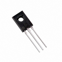
2N4922G ON Semiconductor, 2N4922G Datasheet - Page 4

2N4922G
Manufacturer Part Number
2N4922G
Description
TRANS NPN GP 1A 60V HP TO225AA
Manufacturer
ON Semiconductor
Datasheet
1.2N4923G.pdf
(6 pages)
Specifications of 2N4922G
Transistor Type
NPN
Current - Collector (ic) (max)
1A
Voltage - Collector Emitter Breakdown (max)
60V
Vce Saturation (max) @ Ib, Ic
600mV @ 100mA, 1A
Dc Current Gain (hfe) (min) @ Ic, Vce
30 @ 500mA, 1V
Power - Max
30W
Frequency - Transition
3MHz
Mounting Type
Through Hole
Package / Case
TO-225-3
Transistor Polarity
NPN
Mounting Style
Through Hole
Collector- Emitter Voltage Vceo Max
60 V
Emitter- Base Voltage Vebo
5 V
Maximum Dc Collector Current
1 A
Power Dissipation
30 W
Maximum Operating Temperature
+ 150 C
Continuous Collector Current
3 A
Dc Collector/base Gain Hfe Min
40
Maximum Operating Frequency
3 MHz
Minimum Operating Temperature
- 65 C
Number Of Elements
1
Collector-emitter Voltage
60V
Collector-base Voltage
60V
Emitter-base Voltage
5V
Collector Current (dc) (max)
1A
Dc Current Gain (min)
40
Frequency (max)
3MHz
Operating Temp Range
-65C to 150C
Operating Temperature Classification
Military
Mounting
Through Hole
Pin Count
3
Package Type
TO-225
Lead Free Status / RoHS Status
Lead free / RoHS Compliant
Current - Collector Cutoff (max)
-
Lead Free Status / Rohs Status
Lead free / RoHS Compliant
Other names
2N4922GOS
Available stocks
Company
Part Number
Manufacturer
Quantity
Price
Company:
Part Number:
2N4922G
Manufacturer:
ON Semiconductor
Quantity:
500
7.0
5.0
3.0
2.0
1.0
0.7
0.5
0.3
0.2
0.1
0.07
0.05
10
5.0
3.0
2.0
1.0
0.7
0.5
0.3
0.2
0.1
0.07
0.05
0.03
0.02
0.01
1.0
1.0
0.7
0.5
0.3
0.2
0.1
10
0.01
Figure 5. Active−Region Safe Operating Area
PULSE CURVES APPLY BELOW
0.01
SINGLE PULSE
0.2
0.1
0.05
2.0
D = 0.5
V
I
20
0.02 0.03 0.05
CE
C
/I
RATED V
SECOND BREAKDOWN
LIMITED
BONDING WIRE LIMITED
THERMALLY LIMITED @ T
T
, COLLECTOR−EMITTER VOLTAGE (VOLTS)
B
3.0
J
= 10
T
T
I
t
= 150°C
B1
s
30
J
J
′ = t
= 25°C
= 150°C
I
= I
Figure 6. Storage Time
C
, COLLECTOR CURRENT (mA)
s
B2
CEO
5.0
− 1/8 t
50 70
7.0
I
C
f
/I
5.0 ms
B
= 20
0.1
10
100
dc
C
0.2 0.3
I
C
= 25°C
20
/I
200 300
B
= 20
1.0 ms
30
2N4921, 2N4922, 2N4923
0.5
50
500 700 1000
Figure 4. Thermal Response
100 ms
70
http://onsemi.com
1.0
100
2.0 3.0
t, TIME (ms)
4
q
q
D CURVES APPLY FOR POWER
PULSE TRAIN SHOWN
READ TIME AT t
T
JC
JC
J(pk)
a transistor: average junction temperature and second
breakdown. Safe operating area curves indicate I
operation i.e., the transistor must not be subjected to greater
dissipation than the curves indicate.
is variable depending on conditions. Second breakdown
pulse limits are valid for duty cycles to 10% provided
T
limitations will reduce the power that can be handled to
values less than the limitations imposed by second
breakdown.
(t) = r(t) q
= 4.16°C/W MAX
0.07
0.05
J(pk)
There are two limitations on the power handling ability of
The data of Figure 5 is based on T
5.0
3.0
2.0
1.0
0.7
0.5
0.3
0.2
0.1
− T
5.0
10
C
= P
v 150_C. At high case temperatures, thermal
JC
(pk)
10
1
q
20
JC
(t)
I
C
30
20
/I
B
I
C
= 10
, COLLECTOR CURRENT (mA)
Figure 7. Fall Time
30
50 70
P
I
(pk)
C
50
/I
B
DUTY CYCLE, D = t
= 20
100
t
1
100
t
2
200 300
200 300
J(pk)
T
T
V
I
J
J
B1
CC
1
= 25°C
= 150°C
/t
= I
2
= 30 V
= 150_C; T
B2
500 700 1000
500
C
− V
1000
CE
C


