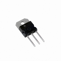
BU323ZG ON Semiconductor, BU323ZG Datasheet - Page 3

BU323ZG
Manufacturer Part Number
BU323ZG
Description
TRANS DARL NPN 350V 10A TO-218
Manufacturer
ON Semiconductor
Datasheet
1.BU323ZG.pdf
(6 pages)
Specifications of BU323ZG
Transistor Type
NPN - Darlington
Current - Collector (ic) (max)
10A
Voltage - Collector Emitter Breakdown (max)
350V
Vce Saturation (max) @ Ib, Ic
1.7V @ 250mA, 10A
Current - Collector Cutoff (max)
100µA
Dc Current Gain (hfe) (min) @ Ic, Vce
500 @ 5A, 4.6V
Power - Max
150W
Frequency - Transition
2MHz
Mounting Type
Through Hole
Package / Case
SOT-93, TO-218 (Straight Leads)
Configuration
Single
Transistor Polarity
NPN
Mounting Style
SMD/SMT
Collector- Emitter Voltage Vceo Max
350 V
Emitter- Base Voltage Vebo
6 V
Maximum Dc Collector Current
10 A
Maximum Collector Cut-off Current
100 uA
Maximum Operating Temperature
+ 175 C
Dc Collector/base Gain Hfe Min
150
Minimum Operating Temperature
- 65 C
Collector Emitter Voltage V(br)ceo
350V
Power Dissipation Pd
150W
Dc Collector Current
10A
Dc Current Gain Hfe
500
Operating Temperature Range
-65°C To +175°C
Rohs Compliant
Yes
Lead Free Status / RoHS Status
Lead free / RoHS Compliant
Available stocks
Company
Part Number
Manufacturer
Quantity
Price
Company:
Part Number:
BU323ZG
Manufacturer:
TOSHIBA
Quantity:
20 000
Company:
Part Number:
BU323ZG
Manufacturer:
ON
Quantity:
30 000
a special high voltage driving circuit. During an
auto−protect cycle, the transistor is turned on again as soon
as a voltage, determined by the zener threshold and the
network, is reached. This prevents the transistor from going
into a Reverse Bias Operating limit condition. Therefore, the
device will have an extended safe operating area and will
always appear to be in “FBSOA.” Because of the built−in
zener and associated network, the I
an unfamiliar shape compared to standard products as
shown in Figure 1.
By design, the BU323Z has a built−in avalanche diode and
I
NOM
= 6.5 A
Icer Leakage Current
I
C
Figure 1. I
Avalanche diode turns on: I
High Voltage Circuit turns on: I
C
Output transistor turns on: I
= f(V
250 V
C
= 100 μA
CE
) Curve Shape
C
C
= 20 mA
300 V
0.001
0.01
= f(V
0.1
10
C
1
= 40 mA
10
340 V
CE
Figure 3. Forward Bias Safe Operating Area
T
C
) curve exhibits
= 25°C
V
V
CLAMP
CE
= 400 V
, COLLECTOR-EMITTER VOLTAGE (VOLTS)
THERMAL LIMIT
SECOND BREAKDOWN LIMIT
CURVES APPLY BELOW
RATED V
V
NOMINAL
CE
http://onsemi.com
CEO
250 ms
3
100
the inductance, are applied according to the Device Under
Test (DUT) specifications. V
test system while making sure the load line remains within
the limits as described in Figure 4.
tested, per the test circuit and criteria described in Figures 2
and 4, to the minimum guaranteed repetitive energy, as
specified in the device parameter section. The device can
sustain this energy on a repetitive basis without degrading
any of the specified electrical characteristics of the devices.
The units under test are kept functional during the complete
test sequence for the test conditions described:
I
R
C(peak)
BE
The bias parameters, V
Note: All BU323Z ignition devices are 100% energy
10 ms
I
B
CURRENT
= 100 Ω, V
SOURCE
1 ms
= 7.0 A, I
Figure 2. Basic Energy Test Circuit
340 V
MERCURY CONTACTS
WETTED RELAY
300 μs
gate
C
H = 5.0 A, I
= 280 V, L = 8.0 mH
R
V
I
BE
B2
BEoff
= 100 Ω
SOURCE
1000
CLAMP
CE
C
and I
L = 100 mA, I
, I
L INDUCTANCE
B1
MONITOR
MONITOR
(8 mH)
(V
C
, V
V
GATE
I
CE
C
are monitored by the
BE(off)
)
, I
B
0.1 Ω
NON
INDUCTIVE
B2
= 100 mA,
I
SOURCE
C
CURRENT
, I
C
, and


