TIP47 ON Semiconductor, TIP47 Datasheet
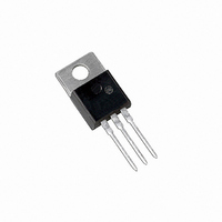
TRANS NPN 1A 250V HI PWR TO220AB

TIP47

Manufacturer Part Number
TIP47
Description
TRANS NPN 1A 250V HI PWR TO220AB
Manufacturer
ON Semiconductor
Datasheet

Specifications of TIP47

Transistor Type
NPN
Current - Collector (ic) (max)
1A
Voltage - Collector Emitter Breakdown (max)
250V
Vce Saturation (max) @ Ib, Ic
1V @ 200mA, 1A
Current - Collector Cutoff (max)
1mA
Dc Current Gain (hfe) (min) @ Ic, Vce
30 @ 300mA, 10V
Power - Max
2W
Frequency - Transition
10MHz
Mounting Type
Through Hole
Package / Case
TO-220-3 (Straight Leads)
Lead Free Status / RoHS Status
Contains lead / RoHS non-compliant
Other names
TIP47OS

Available stocks

Company
Part Number
Manufacturer
Quantity
Price
Part Number:
TIP47
Quantity:
250
Part Number:
TIP47
Manufacturer:
ST
Quantity:
5 000
Part Number:
TIP47
Manufacturer:
ST
Quantity:
20 000
Company:
Part Number:
TIP47
Quantity:
74 850
Part Number:
TIP47C
Manufacturer:
ST
0
Part Number:
TIP47G
Manufacturer:
ON Semiconductor
Quantity:
15
Part Number:
TIP47G
Manufacturer:
ON/安森美
Quantity:
20 000
TIP47G, TIP48G, TIP50G
High Voltage NPN Silicon
Power Transistors
SWITCHMODEt power supply drivers and other switching
applications.
Features
Stresses exceeding Maximum Ratings may damage the device. Maximum
Ratings are stress ratings only. Functional operation above the Recommended
Operating Conditions is not implied. Extended exposure to stresses above the
Recommended Operating Conditions may affect device reliability.
*For additional information on our Pb−Free strategy and soldering details, please
© Semiconductor Components Industries, LLC, 2010
April, 2010 − Rev. 8
MAXIMUM RATINGS
THERMAL CHARACTERISTICS
download the ON Semiconductor Soldering and Mounting Techniques
Reference Manual, SOLDERRM/D.
Collector − Emitter Voltage
Collector − Base Voltage
Emitter − Base Voltage
Collector Current
Base Current
Total Power Dissipation
@ T
Derate above 25_C
Total Power Dissipation
@ T
Derate above 25_C
Unclamped Inducting Load
Energy (See Figure 8)
Operating and Storage
Junction Temperature Range
Thermal Resistance,
Thermal Resistance,
This series is designed for line operated audio output amplifier,
250 V to 400 V (Min) − V
1 A Rated Collector Current
Popular TO−220 Plastic Package
These Devices are Pb−Free and are RoHS Compliant*
Junction−to−Case
Junction−to−Ambient
C
C
= 25_C
= 25_C
Characteristic
− Continuous
− Peak
Rating
CEO(sus)
Symbol
Symbol
T
V
R
R
J
V
V
P
P
CEO
, T
I
I
E
qJC
qJA
CB
EB
C
B
D
D
stg
TIP47
250
350
−65 to +150
TIP48
0.016
3.125
0.32
Max
62.5
300
400
5.0
1.0
2.0
0.6
2.0
40
20
TIP50
400
500
1
W/_C
W/_C
°C/W
°C/W
Unit
Unit
Vdc
Vdc
Vdc
Adc
Adc
mJ
_C
W
W
See detailed ordering and shipping information in the package
dimensions section on page 2 of this data sheet.
1
2
3
POWER TRANSISTORS
250−300− 400 VOLTS
TIPxx
xx
A
Y
WW
G
ORDERING INFORMATION
http://onsemi.com
NPN SILICON
1.0 AMPERE
4
40 WATTS
CASE 221A
TO−220AB
= Device Code
= 47, 48, or 50
= Assembly Location
= Year
= Work Week
= Pb−Free Package
STYLE 1
Publication Order Number:
MARKING
DIAGRAM
TIPxxG
AYWW
TIP47/D

Related parts for TIP47

TIP47 Summary of contents

Page 1

... TIP47G, TIP48G, TIP50G High Voltage NPN Silicon Power Transistors This series is designed for line operated audio output amplifier, SWITCHMODEt power supply drivers and other switching applications. Features • 250 V to 400 V (Min) − V CEO(sus) • Rated Collector Current • Popular TO−220 Plastic Package • ...

Page 2

... Device TIP47 TIP47G TIP48 TIP48G TIP49 TIP49G TIP50 TIP50G (T = 25_C unless otherwise noted) C TIP47 TIP48 TIP50 TIP47 TIP48 TIP50 TIP47 TIP48 TIP50 Package TO−220 TO−220 (Pb−Free) TO−220 TO−220 (Pb−Free) TO−220 TO−220 (Pb−Free) TO−220 TO−220 (Pb−Free) http://onsemi.com 2 Î Î Î Î Î ...

Page 3

TURN-ON PULSE APPROX EB(off APPROX +11 V ≤ 7.0 ...

Page 4

... The data of Figure 5 is based on T variable depending on conditions. Second breakdown pulse limits are valid for duty cycles to 10% provided T v 150_C. T TIP47 Figure 4. At high case temperatures, thermal limitations will TIP48 TIP50 reduce the power that can be handled to values less than the limitations imposed by second breakdown ...

Page 5

T = 150° 25° 55°C 10 6.0 4.0 2.0 0.02 0.04 0.06 0.1 0.2 0 COLLECTOR CURRENT (AMPS) C Figure 9. DC Current Gain 1.4 1.2 1 ...

Page 6

... S 0.045 0.055 1.15 1.39 T 0.235 0.255 5.97 6.47 U 0.000 0.050 0.00 1.27 V 0.045 --- 1.15 --- Z --- 0.080 --- 2.04 PIN 1. BASE 2. COLLECTOR 3. EMITTER 4. COLLECTOR ON Semiconductor Website: www.onsemi.com Order Literature: http://www.onsemi.com/orderlit For additional information, please contact your local Sales Representative TIP47/D ...

Related keywords