MUN5213T1G ON Semiconductor, MUN5213T1G Datasheet
MUN5213T1G
Specifications of MUN5213T1G
Available stocks


Related parts for MUN5213T1G

MUN5213T1G Summary of contents
Page 1
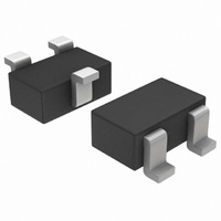
MUN5211T1G Series Bias Resistor Transistor NPN Silicon Surface Mount Transistor with Monolithic Bias Resistor Network This new series of digital transistors is designed to replace a single device and its external resistor bias network. The BRT (Bias Resistor Transistor) contains ...
Page 2
... DEVICE MARKING AND RESISTOR VALUES Device Package MUN5211T1G SC--70/SOT--323 (Pb--Free) MUN5212T1G SC--70/SOT--323 (Pb--Free) MUN5213T1G SC--70/SOT--323 (Pb--Free) MUN5214T1G SC--70/SOT--323 (Pb--Free) MUN5215T1G SC--70/SOT--323 (Pb--Free) MUN5216T1G (Note 3) SC--70/SOT--323 (Pb--Free) MUN5230T1G SC--70/SOT--323 (Pb--Free) MUN5231T1G (Note 3) SC--70/SOT--323 ...
Page 3
... V (BR)CBO V (BR)CEO MUN5211T1G h FE MUN5212T1G MUN5213T1G MUN5214T1G MUN5215T1G MUN5216T1G MUN5230T1G MUN5231T1G MUN5232T1G MUN5233T1G MUN5234T1G MUN5235T1G MUN5236T1G MUN5237T1G V CE(sat) MUN5211T1G MUN5212T1G MUN5213T1G MUN5214T1G MUN5236T1G MUN5230T1G MUN5231T1G MUN5237T1G MUN5215T1G MUN5216T1G MUN5232T1G MUN5233T1G MUN5234T1G MUN5235T1G http://onsemi.com 3 Min Typ Max -- -- 100 nAdc -- -- 500 nAdc ...
Page 4
... MUN5231T1G MUN5232T1G MUN5233T1G MUN5236T1G MUN5237T1G R 1 MUN5211T1G MUN5212T1G MUN5213T1G MUN5214T1G MUN5215T1G MUN5216T1G MUN5230T1G MUN5231T1G MUN5232T1G MUN5233T1G MUN5234T1G MUN5235T1G MUN5236T1G MUN5237T1G MUN5211T1G MUN5212T1G MUN5213T1G MUN5214T1G MUN5215T1G MUN5216T1G MUN5230T1G MUN5231T1G MUN5232T1G MUN5233T1G MUN5234T1G MUN5235T1G MUN5236T1G MUN5237T1G http://onsemi.com 4 Min Typ Max -- -- ...
Page 5
R = 403C/W 50 θ AMBIENT TEMPERATURE (C) A Figure 1. Derating Curve http://onsemi.com 5 100 150 ...
Page 6
TYPICAL ELECTRICAL CHARACTERISTICS - - MUN5211T1G 0.1 0.01 0.001 COLLECTOR CURRENT (mA) C Figure 2. V versus I CE(sat ...
Page 7
TYPICAL ELECTRICAL CHARACTERISTICS - - MUN5212T1G --25C A 0.1 0.01 0.001 COLLECTOR CURRENT (mA) C Figure 7. V versus I CE(sat ...
Page 8
... TYPICAL ELECTRICAL CHARACTERISTICS - - MUN5213T1G --25C A 0.1 0. COLLECTOR CURRENT (mA) C Figure 12. V versus I CE(sat) 1 0.8 0.6 0.4 0 REVERSE BIAS VOLTAGE (VOLTS) R Figure 14. Output Capacitance 100 0.1 0 Figure 16. Input Voltage versus Output Current 1000 25C 100 75 100 MHz 25 0.1 0.01 0.001 ...
Page 9
TYPICAL ELECTRICAL CHARACTERISTICS - - MUN5214T1G 0.1 0.01 0.001 COLLECTOR CURRENT (mA) C Figure 17. V versus I CE(sat) 4 3.5 3 2.5 2 1.5 1 0.5 0 ...
Page 10
TYPICAL ELECTRICAL CHARACTERISTICS — MUN5215T1G 0.1 --25C 25C 0.01 0.001 COLLECTOR CURRENT (mA) C Figure 22. V versus I CE(sat) 4.5 4 3.5 3 2.5 2 1.5 ...
Page 11
TYPICAL ELECTRICAL CHARACTERISTICS — MUN5230T1G 0.1 --25C 25C 0.01 0.001 COLLECTOR CURRENT (mA) C Figure 27. V versus I CE(sat) 4.5 4 3.5 3 2.5 2 1.5 ...
Page 12
TYPICAL ELECTRICAL CHARACTERISTICS — MUN5232T1G 75C 0.1 --25C 25C 0.01 0.001 COLLECTOR CURRENT (mA) C Figure 32. V versus I CE(sat ...
Page 13
TYPICAL ELECTRICAL CHARACTERISTICS — MUN5233T1G 0.1 --25C 25C 0.01 0.001 COLLECTOR CURRENT (mA) C Figure 37. V versus I CE(sat) 4 3.5 3 2.5 2 1.5 1 ...
Page 14
TYPICAL ELECTRICAL CHARACTERISTICS — MUN5235T1G 0.1 --25C 25C 0.01 0.001 COLLECTOR CURRENT (mA) C Figure 42. V versus I CE(sat) 4.5 4 3.5 3 2.5 2 1.5 ...
Page 15
TYPICAL APPLICATIONS FOR NPN BRTs +12 V FROM mP OR OTHER LOGIC Figure 47. Level Shifter: Connects Volt Circuits to Logic V CC OUT IN Figure 48. Open Collector Inverter: Inverts the Input Signal Figure 49. Inexpensive, ...
Page 16
... A1 *For additional information on our Pb--Free strategy and soldering details, please download the ON Semiconductor Soldering and Mounting Techniques Reference Manual, SOLDERRM/D. ON Semiconductor and are registered trademarks of Semiconductor Components Industries, LLC (SCILLC). SCILLC reserves the right to make changes without further notice to any products herein ...