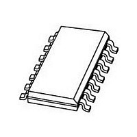
TJA1041T/N1,112 NXP Semiconductors, TJA1041T/N1,112 Datasheet - Page 21

TJA1041T/N1,112
Manufacturer Part Number
TJA1041T/N1,112
Description
Manufacturer
NXP Semiconductors
Datasheet
1.TJA1041TN1112.pdf
(26 pages)
Specifications of TJA1041T/N1,112
Data Rate
1000Kbps
Number Of Transceivers
1
Power Down Mode
Sleep/Standby
Standard Supported
ISO 11898
Operating Supply Voltage (max)
5.25V
Operating Supply Voltage (typ)
5V
Operating Supply Voltage (min)
4.75V
Package Type
SO
Supply Current
80mA
Operating Temperature (max)
150C
Operating Temperature (min)
-40C
Operating Temperature Classification
Automotive
Mounting
Surface Mount
Pin Count
14
Lead Free Status / RoHS Status
Compliant
NXP Semiconductors
15. Soldering
TJA1041_6
Product data sheet
15.1 Introduction to soldering
15.2 Wave and reflow soldering
15.3 Wave soldering
This text provides a very brief insight into a complex technology. A more in-depth account
of soldering ICs can be found in Application Note AN10365 “Surface mount reflow
soldering description” .
Soldering is one of the most common methods through which packages are attached to
Printed Circuit Boards (PCBs), to form electrical circuits. The soldered joint provides both
the mechanical and the electrical connection. There is no single soldering method that is
ideal for all IC packages. Wave soldering is often preferred when through-hole and
Surface Mount Devices (SMDs) are mixed on one printed wiring board; however, it is not
suitable for fine pitch SMDs. Reflow soldering is ideal for the small pitches and high
densities that come with increased miniaturization.
Wave soldering is a joining technology in which the joints are made by solder coming from
a standing wave of liquid solder. The wave soldering process is suitable for the following:
Not all SMDs can be wave soldered. Packages with solder balls, and some leadless
packages which have solder lands underneath the body, cannot be wave soldered. Also,
leaded SMDs with leads having a pitch smaller than ~0.6 mm cannot be wave soldered,
due to an increased probability of bridging.
The reflow soldering process involves applying solder paste to a board, followed by
component placement and exposure to a temperature profile. Leaded packages,
packages with solder balls, and leadless packages are all reflow solderable.
Key characteristics in both wave and reflow soldering are:
Key characteristics in wave soldering are:
•
•
•
•
•
•
•
•
•
•
Through-hole components
Leaded or leadless SMDs, which are glued to the surface of the printed circuit board
Board specifications, including the board finish, solder masks and vias
Package footprints, including solder thieves and orientation
The moisture sensitivity level of the packages
Package placement
Inspection and repair
Lead-free soldering versus PbSn soldering
Process issues, such as application of adhesive and flux, clinching of leads, board
transport, the solder wave parameters, and the time during which components are
exposed to the wave
Solder bath specifications, including temperature and impurities
Rev. 06 — 5 December 2007
High speed CAN transceiver
© NXP B.V. 2007. All rights reserved.
TJA1041
21 of 26


