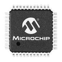
PIC24FV32KA304-E/PT Microchip Technology, PIC24FV32KA304-E/PT Datasheet - Page 68

PIC24FV32KA304-E/PT
Manufacturer Part Number
PIC24FV32KA304-E/PT
Description
32KB Flash, 2KB RAM, 512B EEPROM, 16 MIPS, 12-bit ADC, CTMU, 5V 44 TQFP 10x10x1m
Manufacturer
Microchip Technology
Series
PIC® XLP™ 24Fr
Datasheet
1.PIC24F16KA301T-ISO.pdf
(320 pages)
Specifications of PIC24FV32KA304-E/PT
Processor Series
PIC24FV
Core
PIC
Data Bus Width
16 bit
Program Memory Type
Flash
Program Memory Size
32 KB
Data Ram Size
2 KB
Maximum Operating Temperature
+ 125 C
Mounting Style
SMD/SMT
Package / Case
TQFP-44
Development Tools By Supplier
MPLAB IDE Software
Minimum Operating Temperature
- 40 C
Core Processor
PIC
Core Size
16-Bit
Speed
32MHz
Connectivity
I²C, IrDA, LIN, SPI, UART/USART
Peripherals
Brown-out Detect/Reset, HLVD, POR, PWM, WDT
Number Of I /o
38
Eeprom Size
512 x 8
Ram Size
2K x 8
Voltage - Supply (vcc/vdd)
2 V ~ 5.5 V
Data Converters
A/D 16x12b
Oscillator Type
Internal
Operating Temperature
-40°C ~ 125°C
Lead Free Status / Rohs Status
Details
Available stocks
Company
Part Number
Manufacturer
Quantity
Price
Company:
Part Number:
PIC24FV32KA304-E/PT
Manufacturer:
MICROCHIP
Quantity:
12 000
Company:
Part Number:
PIC24FV32KA304-E/PT
Manufacturer:
Microchip Technology
Quantity:
10 000
- Current page: 68 of 320
- Download datasheet (3Mb)
PIC24FV32KA304 FAMILY
REGISTER 6-1:
DS39995B-page 68
bit 15
bit 7
Legend:
R = Readable bit
-n = Value at POR
bit 15
bit 14
bit 13
bit 12
bit 11-7
bit 6
bit 5-0
R/S-0, HC
WR
U-0
—
WR: Write Control bit (program or erase)
1 = Initiates a data EEPROM erase or write cycle (can be set but not cleared in software)
0 = Write cycle is complete (cleared automatically by hardware)
WREN: Write Enable bit (erase or program)
1 = Enable an erase or program operation
0 = No operation allowed (device clears this bit on completion of the write/erase operation)
WRERR: Flash Error Flag bit
1 = A write operation is prematurely terminated (any MCLR or WDT Reset during programming
0 = The write operation completed successfully
PGMONLY: Program Only Enable bit
1 = Write operation is executed without erasing target address(es) first
0 = Automatic erase-before-write.
Unimplemented: Read as ‘0’
ERASE: Erase Operation Select bit
1 = Perform an erase operation when WR is set
0 = Perform a write operation when WR is set
NVMOP<5:0>: Programming Operation Command Byte bits
Erase Operations (when ERASE bit is ‘1’):
011010 = Erase 8 words
011001 = Erase 4 words
011000 = Erase 1 word
0100xx = Erase entire data EEPROM
Programming Operations (when ERASE bit is ‘0’):
001xx = Write 1 word
ERASE
WREN
R/W-0
R/W-0
operation)
Write operations are preceded automatically by an erase of target address(es).
NVMCON: NONVOLATILE MEMORY CONTROL REGISTER
W = Writable bit
HC = Hardware Clearable bit
‘1’ = Bit is set
NVMOP5
WRERR
R/W-0
R/W-0
PGMONLY
NVMOP4
R/W-0
R/W-0
U = Unimplemented bit, read as ‘0’
S = Settable bit
‘0’ = Bit is cleared
NVMOP3
R/W-0
U-0
—
NVMOP2
R/W-0
U-0
—
2011 Microchip Technology Inc.
x = Bit is unknown
NVMOP1
R/W-0
U-0
—
NVMOP0
R/W-0
U-0
—
bit 8
bit 0
Related parts for PIC24FV32KA304-E/PT
Image
Part Number
Description
Manufacturer
Datasheet
Request
R

Part Number:
Description:
Manufacturer:
Microchip Technology Inc.
Datasheet:

Part Number:
Description:
Manufacturer:
Microchip Technology Inc.
Datasheet:

Part Number:
Description:
Manufacturer:
Microchip Technology Inc.
Datasheet:

Part Number:
Description:
Manufacturer:
Microchip Technology Inc.
Datasheet:

Part Number:
Description:
Manufacturer:
Microchip Technology Inc.
Datasheet:

Part Number:
Description:
Manufacturer:
Microchip Technology Inc.
Datasheet:

Part Number:
Description:
Manufacturer:
Microchip Technology Inc.
Datasheet:

Part Number:
Description:
Manufacturer:
Microchip Technology Inc.
Datasheet:


