SY100S331JZ Micrel Inc, SY100S331JZ Datasheet

IC,FLIP-FLOP,TRIPLE,D TYPE,ECL100,LDCC,28PIN,PLASTIC

SY100S331JZ

Manufacturer Part Number
SY100S331JZ
Description
IC,FLIP-FLOP,TRIPLE,D TYPE,ECL100,LDCC,28PIN,PLASTIC
Manufacturer
Micrel Inc
Series
100Sr
Type
D-Type Busr
Datasheet

Specifications of SY100S331JZ

Rohs Compliant
YES
Function
Master Reset
Output Type
Differential
Number Of Elements
3
Number Of Bits Per Element
1
Frequency - Clock
800MHz
Delay Time - Propagation
300ps
Trigger Type
Positive Edge
Voltage - Supply
4.2 V ~ 5.5 V
Operating Temperature
0°C ~ 85°C
Mounting Type
Surface Mount
Package / Case
28-LCC (J-Lead)
Lead Free Status / RoHS Status
Lead free / RoHS Compliant
Current - Output High, Low
-
Lead Free Status / RoHS Status
Lead free / RoHS Compliant
Other names
576-2475
SY100S331JZ

Available stocks

Company
Part Number
Manufacturer
Quantity
Price
Part Number:
SY100S331JZ
Manufacturer:
Micrel Inc
Quantity:
10 000
Part Number:
SY100S331JZ TR
Manufacturer:
Micrel Inc
Quantity:
10 000
Micrel, Inc.
■ Max. toggle frequency of 800MHz
■ Differential outputs
■ I
■ Industry standard 100K ECL levels
■ Extended supply voltage option:
■ Voltage and temperature compensation for improved
■ Internal 75kΩ input pull-down resistors
■ 150% faster than Fairchild
■ 40% lower power than Fairchild
■ Function and pinout compatible with Fairchild F100K
■ Available in 28-pin PLCC package
M9999-060910
hbwhelp@micrel.com or (408) 955-1690
FEATURES
BLOCK DIAGRAM
V
noise immunity
EE
EE
min. of –80mA
= –4.2V to –5.5V
TRIPLE D
FLIP-FLOP
1
slave flip-flops with true and complement outputs, designed
for use in high-performance ECL systems. Each flip-flop is
controlled by a common clock (CP
pulse (CP
is the logical OR operation of these two clock signals. Data
enters the master when both CP
the slave on the rising edge of either CP
Master Reset (MR) inputs. Each flip-flop also has its own
Direct Set (SD
SD
on this device have 75kΩ pull-down resistors.
DESCRIPTION
PIN NAMES
The SY100S331 offers three D-type, edge-triggered master/
Additional control signals include Master Set (MS) and
CP
CP
D
CD
SD
MR
MS
Q
Q
V
V
n
EES
CCA
0
0
0
and DC
0
c
– D
0
n
– Q
– Q
Pin
– CP
– CD
2
2
2
n
). The resultant clock signal controlling the flip-flop
2
2
n
n
signals override the clock signals. The inputs
) and Direct Clear (CD
Individual Clock Inputs
Common Clock Input
Data Inputs
Individual Direct Clear Inputs
Individual Direct Set Inputs
Master Reset Input
Master Set Input
Data Outputs
Complementary Data Outputs
V
V
EE
CCO
Substrate
for ECL Outputs
c
and CP
Function
c
), as well as its own clock
n
) signals. The MR, MS,
n
c
are LOW and enters
Rev.: I
Issue Date: June 2010
or CP
SY100S331
n
SY100S331
Amendment: /0
(or both).

Related parts for SY100S331JZ

SY100S331JZ Summary of contents

Page 1

Micrel, Inc. FEATURES ■ Max. toggle frequency of 800MHz ■ Differential outputs ■ I min. of –80mA EE ■ Industry standard 100K ECL levels ■ Extended supply voltage option –4.2V to –5.5V EE ■ Voltage and temperature compensation for improved noise immunity ■ Internal 75kΩ input pull-down resistors ■ 150% faster than Fairchild ■ 40% lower power than Fairchild ■ Function and pinout compatible with Fairchild F100K ■ Available in 28-pin PLCC package BLOCK DIAGRAM M9999-060910 hbwhelp@micrel.com or (408) 955-1690 TRIPLE D FLIP-FLOP ...

Page 2

... Undefined Time before CP Positive Transition, t+1 = Time after CP Positive Transition Low-to-High Transition 2 Operating Package Range Marking Commercial SY100S331JC Commercial SY100S331JC Commercial SY100S331JZ with Pb-Free bar-line indicator Commercial SY100S331JZ with Pb-Free bar-line indicator SY100S331JY with Industrial Pb-Free bar-line indicator SY100S331JY with Industrial Pb-Free bar-line indicator (1) Synchronous Operation Inputs ...

Page 3

Micrel, Inc. DC ELECTRICAL CHARACTERISTICS V = –4.2V to –5.5V unless otherwise specified Symbol Parameter I Input HIGH Current, All Inputs IH I Power Supply Current EE AC ELECTRICAL CHARACTERISTICS V = –4.2V to –5.5V unless otherwise specified Symbol ...

Page 4

Micrel, Inc. TIMING DIAGRAMS Note –4.2V to –5.5V unless otherwise specified M9999-060910 hbwhelp@micrel.com or (408) 955-1690 Propagation Delay (Clock) and Transition Times = V = GND CC CCA Propagation Delay (Sets and Resets) 4 SY100S331 ...

Page 5

Micrel, Inc. TIMING DIAGRAMS Notes the minimum time before the transition of the clock that information must be present at the data input the minimum time after the transition of the clock that information must remain ...

Page 6

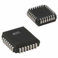
Micrel, Inc. 28-PIN PLCC (J28-1) MICREL, INC. 2180 FORTUNE DRIVE SAN JOSE, CA 95131 USA + 1 (408) 944-0800 tel The information furnished by Micrel in this data sheet is believed to be accurate and reliable. However, no responsibility is assumed by Micrel for its use. Micrel ...

Related keywords