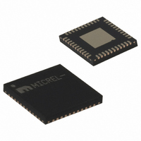
SY56040ARMY TR Micrel Inc, SY56040ARMY TR Datasheet - Page 4

SY56040ARMY TR
Manufacturer Part Number
SY56040ARMY TR
Description
LV CML 4x4 Crosspoint W/o EQ
Manufacturer
Micrel Inc
Datasheet
1.SY56040ARMY.pdf
(14 pages)
Specifications of SY56040ARMY TR
Function
Crosspoint Switch
Circuit
1 x 4:4
Voltage Supply Source
Single Supply
Voltage - Supply, Single/dual (±)
2.375 V ~ 2.625 V, 1.14 V ~ 1.9 V
Operating Temperature
-40°C ~ 85°C
Mounting Type
Surface Mount
Package / Case
44-MLF®, QFN
Lead Free Status / RoHS Status
Lead free / RoHS Compliant
Other names
576-3311-2
Pin Description
September 2008
12,13,20,21,35,
22,25,28,31,34
Pin Number
1,11,14,42
36,43,44
17,15
41,39
23,24
26,27
29,30
32,33
10,8
4,2
16
40
18
19
38
37
9
3
5
7
6
Exposed pad
Pin Name
IN0, /IN0
CONFIG
IN1,/IN1
IN3,/IN3
Q0, /Q0
Q1, /Q1
Q2, /Q2
Q3, /Q3
SOUT0
SOUT1
IN2,/IN
VCCO
LOAD
GND,
SIN0
SIN1
VCC
VT0
VT1
VT2
VT3
NC
Pin Function
Differential Inputs: These input pairs are the differential signal inputs to the device.
They accept differential signals as small as 100mV (200mV
internally terminates with 50Ω to the VT pin. Note that these inputs will default to an
indeterminate state if left open. Please refer to the “Interface Applications” section
for more details.
Input Termination Center-Tap: Each side of the differential input pair terminates to a
VT pin. This pin provides a center-tap to a termination network for maximum
interface flexibility. An internal high impedance resistor divider biases VT to allow
input AC-coupling. For AC-coupling, bypass VT with a 0.1µF low ESR capacitor to
VCC. See “Interface Applications” subsection and Figure 2a.
These single-ended TTL/CMOS-compatible inputs address the data inputs during
switch configuration. Note that this input is internally connected to a 25k ohm pull-
up resistor and will default to a logic HIGH state if left open.
These single-ended TTL/CMOS-compatible inputs address the data outputs during
switch configuration. Note that these inputs are internally connected to a 25kΩ pull-
up resistor and will default to logic HIGH state if left open.
These single-ended TTL/CMOS-compatible inputs control the transfer of the
addresses defined by SIN0/1 and SOUT0/1. See “Switch Configuration,” “Address
Table” and “Timing Diagram” sections for more details. Note that these inputs are
internally connected to a 25kΩ pull-up resistor and will default to logic HIGH state if
left open.
1. Load: Loads configurations into first set of latches. After programming SIN and
2. CONFIG: Loads new configuration into the second set of latches and updates
If the LOAD and CONFIG control signals are floating, one of the output pairs is set
by the programmed SIN and SOUT addresses, as shown in address tables. For the
remaining outputs, setup is random at power up or from previous programmed
states.
CML Differential Output Pairs: Differential buffered copy of the selected input signal.
The output swing is typically 390mV. See “Interface Application” subsection for
termination information.
Positive Power Supply: Bypass with 0.1uF//0.01uF low ESR capacitors as close to
the V
Output Supply: Bypass with 0.1uF//0.01uF low ESR capacitors as close to the V
pins as possible. Supplies the output buffer.
Ground: Exposed pad must be connected to a ground plane that is at the same
potential as the ground pin.
Not Connected.
SOUT with input and output address respectively, pulse the LOAD signal with a
Low to High to Low signal to latch SIN and SOUT. Four LOAD pulses are
needed, each LOAD pulse for each output. See simplified control circuit and
switch configuration description on page 9 for further clarification.
switch configuration. After Loading, pulse CONFIG with a Low to High to Low
signal to load/transfer the latched signal to the output. See simplified control
circuit and switch configuration description on Page 9 for further clarification.
CC
pin as possible. Supplies input and core circuitry.
4
hbwhelp@micrel.com
PP
). Each input pin
or (408) 955-1690
M9999-093008-A
CCO


