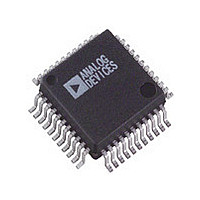
ADV7176AKS Analog Devices Inc, ADV7176AKS Datasheet - Page 9

ADV7176AKS
Manufacturer Part Number
ADV7176AKS
Description
Manufacturer
Analog Devices Inc
Datasheet
1.ADV7176AKS.pdf
(50 pages)
Specifications of ADV7176AKS
Adc/dac Resolution
10b
Screening Level
Commercial
Package Type
MQFP
Pin Count
44
Lead Free Status / RoHS Status
Not Compliant
Available stocks
Company
Part Number
Manufacturer
Quantity
Price
Company:
Part Number:
ADV7176AKS
Manufacturer:
AD
Quantity:
5 510
Company:
Part Number:
ADV7176AKS
Manufacturer:
VIS
Quantity:
5 510
Company:
Part Number:
ADV7176AKS
Manufacturer:
AD
Quantity:
513
Part Number:
ADV7176AKSZ
Manufacturer:
ADI/亚德诺
Quantity:
20 000
CAUTION
ESD (electrostatic discharge) sensitive device. Electrostatic charges as high as 4000 V readily
accumulate on the human body and test equipment and can discharge without detection.
Although the ADV7175A/ADV7176A feature proprietary ESD protection circuitry, permanent
damage may occur on devices subjected to high-energy electrostatic discharges. Therefore,
proper ESD precautions are recommended to avoid performance degradation or loss of functionality.
ABSOLUTE MAXIMUM RATINGS
V
Voltage on Any Digital Input Pin . GND – 0.5 V to V
Storage Temperature (T
Junction Temperature (T
Lead Temperature (Soldering, 10 secs) . . . . . . . . . . . . 260°C
Analog Outputs to GND
NOTES
1
2
Model
ADV7175AKS 0°C to 70°C
ADV7176AKS 0°C to 70°C
Stresses above those listed under Absolute Maximum Ratings may cause permanent
Analog output short circuit to any power supply or common can be of an indefinite
damage to the device. This is a stress rating only; functional operation of the device
at these or any other conditions above those listed in the operational sections of this
specification is not implied. Exposure to absolute maximum rating conditions for
extended periods may affect device reliability.
duration.
AA
to GND . . . . . . . . . . . . . . . . . . . . . . . . . . . . . . . . . . . 7 V
Temperature Package
Range
ORDERING GUIDE
S
2
) . . . . . . . . . . . . . . –65°C to +150°C
J
) . . . . . . . . . . . . . . . . . . . . . . 150°C
. . . . . . . . . . . . . GND – 0.5 to V
Plastic Quad Flatpack S-44
Plastic Quad Flatpack S-44
Description
1
GND
V
P10
P11
P12
V
AA
P5
P6
P7
P8
P9
AA
10
11
1
2
3
4
5
6
7
8
9
12 13 14 15 16 17 18 19 20 21 22
44
PIN 1
IDENTIFIER
43
PIN CONFIGURATION
AA
Package
Option
ADV7175A/ADV7176A
42
+ 0.5 V
41
(Not to Scale)
TOP VIEW
40 39 38
AA
MQFP
PACKAGE THERMAL PERFORMANCE
The 44-MQFP package used for this device takes advantage of
an ADI patented thermal coastline lead frame construction.
This maximizes heat transfer into the leads and reduces the
package thermal resistance.
The junction-to-ambient (θ
four-layer PCB is 35.5°C/W. The junction-to-case thermal
resistance (θ
37
36 35 34
JC
31
33
32
30
29
28
27
26
25
24
23
) is 13.75°C/W.
V
DAC A
GND
DAC B
V
V
DAC D
DAC C
COMP
SDATA
SCLOCK
REF
AA
AA
ADV7175A/ADV7176A
JA
) thermal resistance in still air on a
WARNING!
ESD SENSITIVE DEVICE


