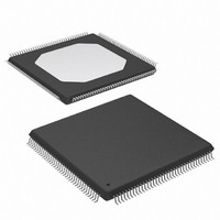
XC3S250E-4TQG144I Xilinx Inc, XC3S250E-4TQG144I Datasheet - Page 142

XC3S250E-4TQG144I
Manufacturer Part Number
XC3S250E-4TQG144I
Description
FPGA Spartan®-3E Family 250K Gates 5508 Cells 572MHz 90nm (CMOS) Technology 1.2V 144-Pin TQFP
Manufacturer
Xilinx Inc
Series
Spartan™-3Er
Datasheet
1.XC3S100E-4VQG100C.pdf
(233 pages)
Specifications of XC3S250E-4TQG144I
Package
144TQFP
Family Name
Spartan®-3E
Device Logic Cells
5508
Device Logic Units
612
Device System Gates
250000
Number Of Registers
4896
Maximum Internal Frequency
572 MHz
Typical Operating Supply Voltage
1.2 V
Maximum Number Of User I/os
108
Ram Bits
221184
Number Of Logic Elements/cells
5508
Number Of Labs/clbs
612
Total Ram Bits
221184
Number Of I /o
108
Number Of Gates
250000
Voltage - Supply
1.14 V ~ 1.26 V
Mounting Type
Surface Mount
Operating Temperature
-40°C ~ 100°C
Package / Case
144-LQFP
Lead Free Status / RoHS Status
Lead free / RoHS Compliant
For Use With
813-1009 - MODULE USB-TO-FPGA TOOL W/MANUAL
Lead Free Status / RoHS Status
Lead free / RoHS Compliant
Available stocks
Company
Part Number
Manufacturer
Quantity
Price
Company:
Part Number:
XC3S250E-4TQG144I
Manufacturer:
XILINX
Quantity:
1 670
Company:
Part Number:
XC3S250E-4TQG144I
Manufacturer:
XILINX
Quantity:
284
Company:
Part Number:
XC3S250E-4TQG144I
Manufacturer:
Xilinx Inc
Quantity:
10 000
Part Number:
XC3S250E-4TQG144I
Manufacturer:
XILINX/赛灵思
Quantity:
20 000
DC and Switching Characteristics
Block RAM Timing
Table 103: Block RAM Timing
142
Notes:
1.
Clock-to-Output Times
T
Setup Times
T
T
T
T
Hold Times
T
T
T
T
Clock Timing
T
T
Clock Frequency
F
Symbol
BCKO
BACK
BDCK
BECK
BWCK
BCKA
BCKD
BCKE
BCKW
BPWH
BPWL
BRAM
The numbers in this table are based on the operating conditions set forth in
When reading from block RAM, the delay from the
active transition at the CLK input to data appearing at
the DOUT output
Setup time for the ADDR inputs before the active
transition at the CLK input of the block RAM
Setup time for data at the DIN inputs before the active
transition at the CLK input of the block RAM
Setup time for the EN input before the active transition
at the CLK input of the block RAM
Setup time for the WE input before the active transition
at the CLK input of the block RAM
Hold time on the ADDR inputs after the active transition
at the CLK input
Hold time on the DIN inputs after the active transition at
the CLK input
Hold time on the EN input after the active transition at
the CLK input
Hold time on the WE input after the active transition at
the CLK input
High pulse width of the CLK signal
Low pulse width of the CLK signal
Block RAM clock frequency. RAM read output value
written back into RAM, for shift-registers and circular
buffers. Write-only or read-only performance is faster.
Description
www.xilinx.com
Table
0.33
0.23
0.67
1.09
0.12
0.12
1.39
1.39
Min
77.
0
0
0
-
-5
Max
2.45
270
Speed Grade
-
-
-
-
-
-
-
-
-
-
DS312-3 (v3.8) August 26, 2009
0.38
0.23
0.77
1.26
0.14
0.13
1.59
1.59
Min
0
0
0
-
-4
Product Specification
Max
2.82
230
-
-
-
-
-
-
-
-
-
-
Units
MHz
ns
ns
ns
ns
ns
ns
ns
ns
ns
ns
ns
R


