IDT71V633S12PF IDT, Integrated Device Technology Inc, IDT71V633S12PF Datasheet
IDT71V633S12PF
Specifications of IDT71V633S12PF
Available stocks


Related parts for IDT71V633S12PF


IDT71V633S12PF Summary of contents
Page 1
... The burst mode feature offers the highest level of performance to the system designer, as the IDT71V633 can provide four cycles of data for a single address presented to the SRAM. An internal burst address counter accepts the first cycle address from the processor, initiating the access sequence. The first cycle of output data will flow-through from the array after a clock-to-data access time delay from the rising clock edge of the same cycle ...
Page 2
... LOW at the rising edge of CLK then BW the circuit. A byte write can still be blocked if ADSP is LOW at the rising edge of CLK. If ADSP is HIGH and BW be written to the SRAM. If BWE is HIGH then the byte write inputs are blocked and only GW can initiate a write cycle. I LOW Synchronous byte write enables ...
Page 3
... IDT71V633, 64K x 32, 3.3V Synchronous SRAM with Flow-Through Outputs Functional Block Diagram LBO ADV CLK ADSC ADSP A – BWE Powerdown OE 32 I/O –I Commercial and Industrial Temperature Ranges Burst CE Sequence 2 Burst Binary Logic Counter Q0 CLR Q1 2 CLK ADDRESS REGISTER 16 Byte 1 Write Register ...
Page 4
... IDT71V633, 64K x 32, 3.3V Synchronous SRAM with Flow-Through Outputs Absolute Maximum DC Ratings Symbol Rating (2) V Terminal Voltage with TERM Respect to GND (3) V Terminal Voltage with TERM Respect to GND T Operating Temperature A T Temperature Under Bias BIAS T Storage Temperature STG P Power Dissipation Output Current ...
Page 5
... IDT71V633, 64K x 32, 3.3V Synchronous SRAM with Flow-Through Outputs Pin Configuration 100 I I DDQ V 5 SSQ SSQ V 11 DDQ DDQ V 21 SSQ SSQ V 27 DDQ I I NOTES 1. Pin 14 does not have to be directly connected Pin 64 can be left unconnected and the device will always remain in active mode. ...
Page 6
... IDT71V633, 64K x 32, 3.3V Synchronous SRAM with Flow-Through Outputs Synchronous Truth Table Address Operation Deselected Cycle, Power Down Deselected Cycle, Power Down Deselected Cycle, Power Down Deselected Cycle, Power Down Deselected Cycle, Power Down Read Cycle, Begin Burst Read Cycle, Begin Burst ...
Page 7
... IDT71V633, 64K x 32, 3.3V Synchronous SRAM with Flow-Through Outputs Synchronous Write Function Truth Table GW Operation Read H Read H Write all Bytes L Write all Bytes H (2) Write Byte 1 H (2) Write Byte 2 H (2) Write Byte 3 H (2) Write Byte 4 H NOTES Don’t Care Multiple bytes may be selected during the same cycle. ...
Page 8
... IDT71V633, 64K x 32, 3.3V Synchronous SRAM with Flow-Through Outputs DC Electrical Characteristics Over the Operating Temperature and Supply Voltage Range Symbol Parameter |I | Input Leakage Current LI ZZ & LBO Input Leakage Current | Output Leakage Current | LO V Output Low Voltage OL V Output High Voltage ...
Page 9
... IDT71V633, 64K x 32, 3.3V Synchronous SRAM with Flow-Through Outputs AC Electrical Characteristics (V = 3.3V +10/-5%, Commercial and Industrial Temperature Ranges) DD Symbol Clock Parameters t Clock Cycle Time CYC (1) t Clock High Pulse Width CH (1) t Clock Low Pulse Width CL Output Parameters t Clock High to Valid Data ...
Page 10
... IDT71V633, 64K x 32, 3.3V Synchronous SRAM with Flow-Through Outputs Timing Waveform of Read Cycle Commercial and Industrial Temperature Ranges (1, ...
Page 11
... IDT71V633, 64K x 32, 3.3V Synchronous SRAM with Flow-Through Outputs Timing Waveform of Combined Read and Write Cycles Commercial and Industrial Temperature Ranges (1,2,3) 11 6.42 . ...
Page 12
... IDT71V633, 64K x 32, 3.3V Synchronous SRAM with Flow-Through Outputs Timing Waveform of Write Cycle No. 1 — GW Controlled Commercial and Industrial Temperature Ranges (1,2, ...
Page 13
... IDT71V633, 64K x 32, 3.3V Synchronous SRAM with Flow-Through Outputs Timing Waveform of Write Cycle No. 2 — Byte Controlled Commercial and Industrial Temperature Ranges 13 6.42 (1,2,3) . ...
Page 14
... IDT71V633, 64K x 32, 3.3V Synchronous SRAM with Flow-Through Outputs Timing Waveform of Sleep (ZZ) and Power-Down Modes Commercial and Industrial Temperature Ranges (1,2, ...
Page 15
... IDT71V633, 64K x 32, 3.3V Synchronous SRAM with Flow-Through Outputs Non-Burst Read Cycle Timing Waveform CLK ADSP ADSC ADDRESS Av GW, BWE, BWx CE DATA OUT NOTES input is LOW, ADV is HIGH, and LBO is Don’t Care for this cycle. 2. (Ax) represents the data for address Ax, etc. ...
Page 16
... IDT71V633, 64K x 32, 3.3V Synchronous SRAM with Flow-Through Outputs Non-Burst Write Cycle Timing Waveform CLK ADSP ADSC ADDRESS DATA IN NOTES input is LOW, ADV and OE are HIGH, and LBO is Don't Care for this cycle. 2. (Ax) represents the data for address Ax, etc. ...
Page 17
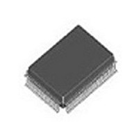
... IDT71V633, 64K x 32, 3.3V Synchronous SRAM with Flow-Through Outputs 100-pin Thin Quad Plastic Flatpack (TQFP) Package Diagram Outline Commercial and Industrial Temperature Ranges 17 6.42 ...
Page 18
... IDT71V633, 64K x 32, 3.3V Synchronous SRAM with Flow-Through Outputs Ordering Information IDT 71V633 S X Device Power Speed Type PART NUMBER SPEED IN MEGAHERTZ 71V633S11PF 71V633S12PF PF X Package Process/ Temperature Range Blank Commercial only. t PARAMETER CD 50 MHz MHz Commercial and Industrial Temperature Ranges Commercial (0° ...
Page 19
... IDT71V633, 64K x 32, 3.3V Synchronous SRAM with Flow-Through Outputs Datasheet Document History 9/9/99 Pg. 6–8 Pg. 10–14 Pg. 18 9/30/99 Pg 10/8/99 Pg. 1 04/04/00 Pg. 17 08/09/00 08/17/01 CORPORATE HEADQUARTERS 6024 Silver Creek Valley Road San Jose, CA 95138 The IDT logo is a registered trademark of Integrated Device Technology, Inc. ...