HDSP2114S OSRAM Opto Semiconductors Inc, HDSP2114S Datasheet - Page 12
HDSP2114S
Manufacturer Part Number
HDSP2114S
Description
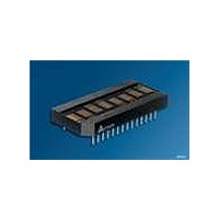
LED Displays 5x7 Hi-Eff Green 0.2 , 8-CHARACTER
Manufacturer
OSRAM Opto Semiconductors Inc
Series
Intelligent Display®r
Datasheet
1.HDSP2110S.pdf
(16 pages)
Specifications of HDSP2114S
Display Type
Dot Matrix
Emitting Color
Hi-Eff. Green
Number Of Digits
8
Digit Size (in)
.2in
Viewing Area Height (mm)
4.81mm
Viewing Area Length (mm)
2.85mm
Package Type
Panel
Operating Supply Voltage (min)
4.5V
Operating Supply Voltage (typ)
5V
Operating Supply Voltage (max)
5.5V
Operating Temperature Classification
Industrial
Operating Temp Range
-40C to 85C
Mounting
Through Hole
Pin Count
28
Total Thickness (mm)
5.31mm
Opto Display Type
Panel
Pattern Type
Dot Matrix
Millicandela Rating
200µcd
Size / Dimension
1.70" L x 0.77" W x 0.21" H (42.67mm x 19.58mm x 5.31mm)
Color
Green
Configuration
5 x 7
Character Size
0.2 in
Illumination Color
High Efficiency Green
Wavelength
568 nm
Maximum Operating Temperature
+ 85 C
Minimum Operating Temperature
- 40 C
Luminous Intensity
510 ucd
Viewing Area (w X H)
2.85 mm x 4.81 mm
Lead Free Status / RoHS Status
Compliant
Voltage - Forward (vf) Typ
-
Internal Connection
-
Lead Free Status / Rohs Status
Details
Other names
Q68000A8564
Available stocks
Company
Part Number
Manufacturer
Quantity
Price

Part Number:
HDSP2114S-24
Manufacturer:
SIEMENS/西门子
Quantity:
20 000


Blink Function
Control Word bit, D4, enables or disables the Blink Function. When
D4 is 1, the Blink Function is enabled and all characters on the dis-
play will blink at approximately 2.0 Hz. The Blink Function will over-
ride the Flash Function if both functions are enabled. When D4 is 0,
the Blink Function is disabled. When using an external clock, the
blink rate can be determined by dividing the clock rate by 28,672.
For synchronized blinking on multiple displays, see the Reset Sec-
tion.
Self Test
Before starting Self Test, Reset must first be activated. Control
Word bits, D6 and D5, are used for the Self Test Function. When
D6 is 1, the Self Test is initiated. Results of the Self Test are stored
in bits D5. Control Word bit, D5, is a read only bit. When D5 is 1,
Self Test passed is indicated. When D5 is 0, Self Test failed is indi-
cated. The Self Test function of the IC consists of two internal rou-
tines which exercise major portions of the IC and illuminates all of
the LEDs. The first routine cycles the ASCII decoder ROM through
all states and performs a check sum on the output. If the check
sum agrees with the correct value, D5 is set to a 1.
UDC Character Map
Flash RAM Access Logic
RST
1
1
Control Word Access Logic
RST
1
1
2006-01-23
Row Data
A2
0
0
0
0
1
1
1
HSDP2110S, HSDP2111S, HSDP2112S, HSDP2113S, HSDP2114S, HSDP2115S
A1
0
0
1
1
0
0
1
CE
0
0
CE
0
0
A0
0
1
0
1
0
1
0
WR
0
1
WR
0
1
Row #
1
2
3
4
5
6
7
RD
1
0
RD
1
0
FL
0
0
FL
1
1
Column Data
C1
D4
5 x 7
Dot Matrix
Pattern
A4
X
X
A4
1
1
C2
D3
A3
X
X
A3
0
0
C3
D2
C4
D1
A2
Flash RAM Address
for Digits 0–7
Flash RAM Address
for Digits 0–7
A2
Not used for Control Word Control Word data for a Write Cycle,
Not used for Control Word Control Word data for a Read during a Read Cycle
C5
D0
A1
A1
A0
A0
12
The second routine provides a visual test of the LEDs using the
drive circuitry. This is accomplished by writing checkered and
inverse checkered patterns to the display. Each pattern is dis-
played for approximately 2.0 seconds. During the self test function
the display must not be accessed. The time needed to execute the
self test function is calculated by multiplying the clock time by
262,144 (typical time = 4.6 sec.). At the end of the self test func-
tion, the Character RAM is loaded with blanks; the Control Word
Register is set to zeroes except D5, and the Flash RAM is cleared
and the UDC Address Register is set to all 1.0 s.
Clear Function (see Table „Clear Function“ (page 13) and Figure
„Control Word Data Definition“ (page 13))
Control Word bit, D7 clears the character RAM to 20 hex and the
flash RAM to all zeroes. The RAMs are cleared within three clock
cycles (110 µs minimum, using the internal clock) when D7 is set
to 1. During the clear time the display must not be accessed.
When the clear function is finished, bit 7 of the
Control Word RAM will be reset to a “0”.
Reset Function
The display should be reset on power up of the display
(RST=LOW). When the display is reset, the Character RAM, Flash
RAM, and Control Word Register are cleared.
The display's internal counters are reset. Reset cycle takes three
clock cycles (110 µseconds minimum using the internal clock).The
display must not be accessed during this time.
To synchronize the flashing and blinking of multiple displays, it is
necessary for the display to use a common clock source and reset
all the displays at the same time to start the internal counters at
the same place.
While RST is low, the display must not be accessed by RD nor
WR.
D7 D6 D5 D4 D3 D2 D1 D0
D0=Flash Data, 0-Flash Off and 1=Flash On (Write Cycle)
D0=Flash Data, 0-Flash Off and 1=Flash On (Read Cycle)
D7 D6 D5 D4 D3 D2 D1 D0
see Figure „Control Word Data Definition“ (page 13)
Related parts for HDSP2114S
Image
Part Number
Description
Manufacturer
Datasheet
Request
R

Part Number:
Description:
INTELLIGENT DISP 4CHAR 5X7 HERED
Manufacturer:
OSRAM Opto Semiconductors Inc
Datasheet:

Part Number:
Description:
DISPLAY 8DIGIT CERAMIC GREEN
Manufacturer:
OSRAM Opto Semiconductors Inc
Datasheet:

Part Number:
Description:
EMITTER IR 950NM 5MM SMD RADIAL
Manufacturer:
OSRAM Opto Semiconductors Inc
Datasheet:

Part Number:
Description:
LED TOPLED GREEN 570NM 2-PLCC
Manufacturer:
OSRAM Opto Semiconductors Inc
Datasheet:

Part Number:
Description:
INTERRUPTER RELFECT W/FILTR SMD
Manufacturer:
OSRAM Opto Semiconductors Inc
Datasheet:

Part Number:
Description:
LED Displays 5x7 Green 0.145 , 4-CHARACTER
Manufacturer:
OSRAM Opto Semiconductors Inc
Datasheet:

Part Number:
Description:
Q65110A4321_SIDELED PURE GREEN EOL150407
Manufacturer:
OSRAM Opto Semiconductors Inc
Datasheet:
Part Number:
Description:
Q65110A1202_RO DETECTOR 3/5MM_TR_RO
Manufacturer:
OSRAM Opto Semiconductors Inc
Datasheet:

Part Number:
Description:
PHOTODIODE 900NM 3MM W/FILTER
Manufacturer:
OSRAM Opto Semiconductors Inc
Datasheet:
Part Number:
Description:
INTELLIGENT DISP 4CHAR 5X7 HERED
Manufacturer:
OSRAM Opto Semiconductors Inc
Datasheet:
Part Number:
Description:
LED TOPLED GREEN 570NM 2-PLCC
Manufacturer:
OSRAM Opto Semiconductors Inc
Datasheet:
Part Number:
Description:
PHOTODIODE 900NM 3MM W/FILTER
Manufacturer:
OSRAM Opto Semiconductors Inc
Datasheet:

Part Number:
Description:
PHOTODIODE 850NM THRU-HOLE
Manufacturer:
OSRAM Opto Semiconductors Inc
Datasheet:

Part Number:
Description:
PHOTODIODE 880NM W/FILTER SMD
Manufacturer:
OSRAM Opto Semiconductors Inc
Datasheet: