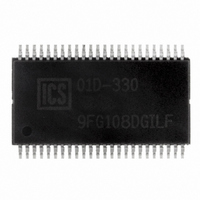
ICS9FG108DGILFT IDT, Integrated Device Technology Inc, ICS9FG108DGILFT Datasheet

ICS9FG108DGILFT
Specifications of ICS9FG108DGILFT
9FG108DGILFT
Available stocks
Related parts for ICS9FG108DGILFT
ICS9FG108DGILFT Summary of contents
Page 1
Frequency Generator for CPU, QPI, FBD, PCIe Gen 2 & SATA Description ICS9FG108D is a Frequency Timing Generator that provides 8 differential output pairs that are compliant to the Intel CK410 specification. It also provides support for PCI-Express, next generation ...
Page 2
ICS9FG108D Frequency Generator for CPU, QPI, FBD, PCIe Gen 2 & SATA Pin Configuration XIN/CLKIN VDD 3 GND 4 REFOUT 5 vFS2 6 vOE_7 7 DIF_7 8 DIF_7# 9 VDD 10 DIF_6 11 DIF_6# 12 ^OE_6 13 ...
Page 3
ICS9FG108D Frequency Generator for CPU, QPI, FBD, PCIe Gen 2 & SATA Pin Description PIN # PIN PIN TYPE 1 XIN /C LKIN PWR PWR 5 ...
Page 4
ICS9FG108D Frequency Generator for CPU, QPI, FBD, PCIe Gen 2 & SATA Pin Description (continued) PIN # PIN NAME PIN TYPE 25 DIF_STOP vSPREAD IN 27 ^SEL14M_25M vOE_3 IN 29 DIF_3# OUT 30 DIF_3 OUT 31 ...
Page 5
ICS9FG108D Frequency Generator for CPU, QPI, FBD, PCIe Gen 2 & SATA Absolute Max Symbol Parameter VDD_A 3.3V Core Supply Voltage VDD 3.3V Logic Supply Voltage Ts Storage Temperature Tambient Ambient Operating Temp•(Commerical Grade) Tambient Ambient Operating Temp•(Industrial Grade) Tcase ...
Page 6
ICS9FG108D Frequency Generator for CPU, QPI, FBD, PCIe Gen 2 & SATA Electrical Characteristics - Input/Supply/Common Output Parameters T = Tambient, Supply Voltage V = 3.3 V +/- PARAMETER SYMBOL Input High Voltage V IH Input Low Voltage ...
Page 7
ICS9FG108D Frequency Generator for CPU, QPI, FBD, PCIe Gen 2 & SATA Electrical Characteristics - DIF 0.7V Current Mode Differential Pair T = Tambient, Supply Voltage VDD = 3.3 V +/-5 =49.9 Ω 475 Ω ...
Page 8
ICS9FG108D Frequency Generator for CPU, QPI, FBD, PCIe Gen 2 & SATA General SMBus serial interface information for the ICS9FG108D How to Write: • Controller (host) sends a start bit. • Controller (host) sends the write address DC • ICS ...
Page 9
ICS9FG108D Frequency Generator for CPU, QPI, FBD, PCIe Gen 2 & SATA SMBus Table: Device Control Register, READ/WRITE ADDRESS (DC/DD) Byte 0 Pin # Name 27 Bit 7 5 Bit 6 Bit 5 44 Bit Bit 3 ...
Page 10
ICS9FG108D Frequency Generator for CPU, QPI, FBD, PCIe Gen 2 & SATA SMBus Table: Frequency Select Readback Register Byte 3 Pin # Name SEL14M_25M# 27 Bit 7 (FS3) 6 Bit 6 FS2 44 Bit 5 FS1 45 Bit 4 FS0 ...
Page 11
ICS9FG108D Frequency Generator for CPU, QPI, FBD, PCIe Gen 2 & SATA SMBus Table: Byte Count Register Byte 6 Pin # Name Bit 7 - BC7 Bit 6 - BC6 Bit 5 - BC5 Bit 4 - BC4 Bit 3 ...
Page 12
ICS9FG108D Frequency Generator for CPU, QPI, FBD, PCIe Gen 2 & SATA SMBus Table: PLL Frequency Control Register Byte 10 Pin # Name - PLL N Div8 Bit 7 - PLL N Div9 Bit 6 - PLL M Div5 Bit ...
Page 13
ICS9FG108D Frequency Generator for CPU, QPI, FBD, PCIe Gen 2 & SATA DIF_STOP# - Assertion (transition from '1' to '0') Asserting DIF_STOP# pin stops all DIF outputs that are set to be stoppable after their next transition. When the SMBus ...
Page 14
ICS9FG108D Frequency Generator for CPU, QPI, FBD, PCIe Gen 2 & SATA Common Recommendations for Differential Routing L1 length, route as non-coupled 50ohm trace L2 length, route as non-coupled 50ohm trace L3 length, route as non-coupled 50ohm trace Rs Rt ...
Page 15
ICS9FG108D Frequency Generator for CPU, QPI, FBD, PCIe Gen 2 & SATA Alternative Termination for LVDS and other Common Differential Signals (figure 3) Vdiff Vp-p Vcm 0.45v 0.22v 1.08 0.58 0.28 0.6 0.80 0.40 0.6 0.60 0.3 1.2 R1a = ...
Page 16
ICS9FG108D Frequency Generator for CPU, QPI, FBD, PCIe Gen 2 & SATA 48-pin SSOP Package Outline and Dimensions INDEX INDEX AREA AREA 45° SEATING SEATING b PLANE PLANE .10 ...
Page 17
ICS9FG108D Frequency Generator for CPU, QPI, FBD, PCIe Gen 2 & SATA 48-pin TSSOP Package Outline and Dimensions INDEX INDEX AREA AREA aaa Ordering Information Part / ...
Page 18
ICS9FG108D Frequency Generator for CPU, QPI, FBD, PCIe Gen 2 & SATA Revision History Rev. Issue Date Description 0.1 12/18/2008 New datasheet. 1. Updated phase jitter tables. 2, Updated input frequency ranges. There are now separate ranges for 14.318M input ...


