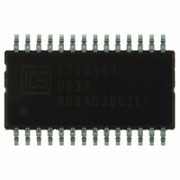
ICS9DB403DGILFT IDT, Integrated Device Technology Inc, ICS9DB403DGILFT Datasheet
ICS9DB403DGILFT
Specifications of ICS9DB403DGILFT
9DB403DGILFT
Available stocks


Related parts for ICS9DB403DGILFT


ICS9DB403DGILFT Summary of contents
Page 1
Four Output Differential Buffer for PCIe Gen 1 and Gen 2 Description The ICS9DB403 is compatible with the Intel DB400v2 Differential Buffer Specification. This buffer provides 4 PCI-Express Gen2 clocks. The ICS9DB403 is driven by a differential output pair from ...
Page 2
ICS9DB403D Four Output Differential Buffer for PCIe for Gen 1 and Gen 2 Pin Configuration VDD 1 SRC_IN 2 SRC_IN# 3 GND 4 VDD 5 DIF_1 6 DIF_1# 7 OE_1 8 DIF_2 9 DIF_2# 10 VDD 11 BYPASS#/PLL 12 SCLK ...
Page 3
ICS9DB403D Four Output Differential Buffer for PCIe for Gen 1 and Gen 2 Pin Decription When OE_INV = 0 PIN # PIN NAME PIN TYPE 1 VDD PWR 2 SRC_IN IN 3 SRC_IN GND PWR 5 VDD PWR ...
Page 4
ICS9DB403D Four Output Differential Buffer for PCIe for Gen 1 and Gen 2 Pin Decription When OE_INV = 1 PIN # PIN NAME PIN TYPE 1 VDD PWR 2 SRC_IN IN 3 SRC_IN GND PWR 5 VDD PWR ...
Page 5
ICS9DB403D Four Output Differential Buffer for PCIe for Gen 1 and Gen 2 Absolute Max Symbol Parameter VDD_A 3.3V Core Supply Voltage VDD_In 3.3V Logic Supply Voltage V Input Low Voltage IL V Input High Voltage IH Ts Storage Temperature ...
Page 6
ICS9DB403D Four Output Differential Buffer for PCIe for Gen 1 and Gen 2 Electrical Characteristics - Input/Supply/Common Output Parameters T = Tambient for the desired operating range, Supply Voltage V A PARAMETER SYMBOL V Input High Voltage IHSE V Input ...
Page 7
ICS9DB403D Four Output Differential Buffer for PCIe for Gen 1 and Gen 2 Electrical Characteristics - DIF 0.7V Current Mode Differential Pair T =Tambient 3.3 V +/-5 PARAMETER SYMBOL Current Source Output Zo Impedance Voltage ...
Page 8
ICS9DB403D Four Output Differential Buffer for PCIe for Gen 1 and Gen 2 Clock Periods Differential Outputs with Spread Spectrum Enabled Measurement Window 1 Clock Symbol Lg- Absolute Short-term Period Average Definition Minimum Minimum Absolute Absolute Period Period DIF 100 ...
Page 9
ICS9DB403D Four Output Differential Buffer for PCIe for Gen 1 and Gen 2 Common Recommendations for Differential Routing L1 length, route as non-coupled 50ohm trace L2 length, route as non-coupled 50ohm trace L3 length, route as non-coupled 50ohm trace Rs ...
Page 10
ICS9DB403D Four Output Differential Buffer for PCIe for Gen 1 and Gen 2 Alternative Termination for LVDS and other Common Differential Signals (figure 3) Vdiff Vp-p Vcm 0.45v 0.22v 1.08 0.58 0.28 0.6 0.80 0.40 0.6 0.60 0.3 1.2 R1a ...
Page 11
ICS9DB403D Four Output Differential Buffer for PCIe for Gen 1 and Gen 2 General SMBus serial interface information for the ICS9DB403D How to Write: • Controller (host) sends a start bit. • Controller (host) sends the write address DC • ...
Page 12
ICS9DB403D Four Output Differential Buffer for PCIe for Gen 1 and Gen 2 SMBus Table: Frequency Select Register, READ/WRITE ADDRESS (DC/DD) Byte 0 Pin # Name Bit 7 - PD_Mode Bit 6 - STOP_Mode Bit 5 - PD_Polarity Bit 4 ...
Page 13
ICS9DB403D Four Output Differential Buffer for PCIe for Gen 1 and Gen 2 SMBus Table: Vendor & Revision ID Register Byte 4 Pin # Name Bit 7 - RID3 Bit 6 - RID2 Bit 5 - RID1 Bit 4 - ...
Page 14
ICS9DB403D Four Output Differential Buffer for PCIe for Gen 1 and Gen 2 Note: Polarities in timing diagrams are shown OE_INV = 0. They are similar to OE_INV = 1. PD#, Power Down The PD# pin cleanly shuts off all ...
Page 15
ICS9DB403D Four Output Differential Buffer for PCIe for Gen 1 and Gen 2 SRC_STOP# The SRC_STOP# signal is an active-low asynchronous input that cleanly stops and starts the DIF outputs. A valid clock must be present on SRC_IN for this ...
Page 16
ICS9DB403D Four Output Differential Buffer for PCIe for Gen 1 and Gen 2 SRC_STOP_3 (SRC_Stop = Driven Tristate) SRC_Stop# PWRDWN# DIF (Free Running) DIF# (Free Running) DIF (Stoppable) DIF# (Stoppable) SRC_STOP_4 (SRC_Stop = Tristate Tristate) SRC_Stop# ...
Page 17
ICS9DB403D Four Output Differential Buffer for PCIe for Gen 1 and Gen 2 28-pin SSOP Package Dimensions 209 mil SSOP Four Output Differential Buffer for PCIe Gen 1 and Gen IDT /ICS 209 mil SSOP In Millimeters ...
Page 18
ICS9DB403D Four Output Differential Buffer for PCIe for Gen 1 and Gen 2 28-pin TSSOP Package Dimensions INDEX INDEX AREA AREA aaa Ordering Information Part / Order ...
Page 19
ICS9DB403D Four Output Differential Buffer for PCIe Gen 1 and Gen 2 Revision History Rev. Issue Date Description 1. Updated electrical characteristics for final data sheet A 8/15/2006 2. Corrected references to 8 outputs (should 5/22/2007 Updated ...