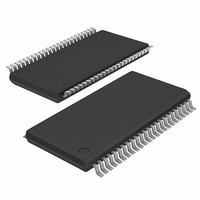
ICS95V157AG IDT, Integrated Device Technology Inc, ICS95V157AG Datasheet

ICS95V157AG
Specifications of ICS95V157AG
Related parts for ICS95V157AG
ICS95V157AG Summary of contents
Page 1
Integrated Circuit Systems, Inc. 2.5V Single-Ended to SSTL_2 Clock Driver (45MHz - 233MHz) Recommended Application: Single-ended clock input with zero delay board fan out Product Description/Features: • Low skew, low jitter PLL clock driver • differential clock ...
Page 2
ICS95V157 Pin Descriptions ...
Page 3
Absolute Maximum Ratings Supply Voltage (VDD & AVDD -0.5V to 4.6V Logic Inputs . . . . . . . . . . . . . . . . ...
Page 4
ICS95V157 Recommended Operating Condition (see note1 85°C; Supply Voltage AVDD, VDD = 2.5 V +/- 0.2V (unless otherwise stated) A PARAMETER SYMBOL Supply Voltage Low level input voltage V IL High level ...
Page 5
Timing Requirements 85°C; Supply Voltage A A VDD PARAMETER SYMBOL Max clock frequency Application Frequency Range Input clock duty cycle CLK stabilization Switching Characteristics (see note 3) PARAMETER Low-to high level propagation delay time High-to low ...
Page 6
ICS95V157 Y , FB_OUTC FB_OUTT X 0501C—11/24/08 6 ...
Page 7
CLK_INC CLK_INT FB_INC FB_INT FB_OUTC FB_OUTT FB_OUTC FB_OUTT FB_OUTC FB_OUTT X 0501C—11/24/08 Parameter Measurement Information ...
Page 8
ICS95V157 Y , FB_OUTC FB_OUTT X 20% Clock Inputs and Outputs 0501C—11/24/08 Parameter Measurement Information t (hper_n) t (hper_n+ (jit_Hper) (jit_Hper_n) 2xf O Figure 7. Half-Period Jitter 80% Rise ...
Page 9
INDEX INDEX AREA AREA aaa 6.10 mm. Body, 0.50 mm. pitch TSSOP (20 mil) (240 mil) Ordering Information 95V157yG - T Example: XXXX ...


