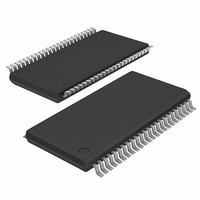
ICS9DB801BGLF IDT, Integrated Device Technology Inc, ICS9DB801BGLF Datasheet

ICS9DB801BGLF
Specifications of ICS9DB801BGLF
Available stocks
Related parts for ICS9DB801BGLF
ICS9DB801BGLF Summary of contents
Page 1
Integrated Circuit Systems, Inc. Eight Output Differential Buffer for PCI Express (50-200MHz) Recommended Application: DB800 Version 2.0 Yellow Cover part with PCI Express suppor with extended bypass mode frequency range. Output Features: • 0.7V current-mode differential output pairs ...
Page 2
Integrated Circuit Systems, Inc. Pin Desription for OE_INV = 0 PIN PIN # PIN NAME TYPE 1 SRC_DIV VDD PWR 3 GND PWR 4 SRC_IN IN 5 SRC_IN OE_0 IN 7 OE_3 IN 8 DIF_0 OUT ...
Page 3
Integrated Circuit Systems, Inc. Pin Desription for OE_INV = 0 PIN PIN # PIN NAME TYPE 25 GND PWR 26 PD SRC_STOP HIGH_BW DIF_4# OUT 30 DIF_4 OUT 31 VDD PWR 32 GND PWR ...
Page 4
Integrated Circuit Systems, Inc. Pin Desription for OE_INV = 1 PIN # PIN NAME PIN TYPE 1 SRC_DIV# 2 VDD PWR 3 GND PWR 4 SRC_IN 5 SRC_IN# 6 OE0# 7 OE3# 8 DIF_0 OUT 9 DIF_0# OUT 10 GND ...
Page 5
Integrated Circuit Systems, Inc. Pin Desription for OE_INV = 1 PIN # PIN NAME PIN TYPE 25 GND PWR SRC_STOP IN 28 HIGH_BW DIF_4# OUT 30 DIF_4 OUT 31 VDD PWR 32 GND PWR ...
Page 6
Integrated Circuit Systems, Inc. General Description The ICS9DB801 follows the Intel DB800 Differential Buffer Specification v2.0. This buffer provides eight PCI-Express SRC clocks. The ICS9DB801 is driven by a differential input pair from a CK409/CK410 main clock generator, such as ...
Page 7
Integrated Circuit Systems, Inc. Absolute Max Symbol Parameter VDD_A 3.3V Core Supply Voltage VDD_In 3.3V Logic Supply Voltage V Input Low Voltage IL V Input High Voltage IH Ts Storage Temperature Tambient Ambient Operating Temp Tcase Case Temperature Input ESD ...
Page 8
Integrated Circuit Systems, Inc. Electrical Characteristics - DIF 0.7V Current Mode Differential Pair 70° 3.3 V +/-5%; C =2pF PARAMETER SYMBOL Current Source Output Zo Impedance Voltage High VHigh Voltage ...
Page 9
Integrated Circuit Systems, Inc. Common Recommendations for Differential Routing L1 length, Route as non L2 length, Route as non L3 length, Route as non Rs Rt Down Device Differential Routing L4 length, Route as coupled differential trace. L4 length, Route ...
Page 10
Integrated Circuit Systems, Inc. General SMBus serial interface information for the ICS9DB801 How to Write: • Controller (host) sends a start bit. • Controller (host) sends the write address DC • ICS clock will acknowledge • Controller (host) sends the ...
Page 11
Integrated Circuit Systems, Inc. SMBus Table: Frequency Select Register, READ/WRITE ADDRESS (DC/DD) Byte 0 Pin # Name Bit 7 - PD_Mode - Bit 6 STOP_Mode Bit 5 - Reserved - Bit 4 Reserved - Bit 3 Reserved - Bit 2 ...
Page 12
Integrated Circuit Systems, Inc. SMBus Table: Output Control Register Byte 3 Pin # Name Bit 7 Bit 6 Bit 5 Bit 4 Bit 3 Bit 2 Bit 1 Bit 0 SMBus Table: Vendor & Revision ID Register Byte 4 Pin ...
Page 13
Integrated Circuit Systems, Inc. Note: Polarities in timing diagrams are shown OE_INV = 0. They are similar to OE_INV = 1. PD#, Power Down The PD# pin cleanly shuts off all clocks and places the device into a power saving ...
Page 14
Integrated Circuit Systems, Inc. SRC_STOP# The SRC_STOP# signal is an active-low asynchronous input that cleanly stops and starts the DIF outputs. A valid clock must be present on SRC_IN for this input to work properly. The SRC_STOP# signal is de-bounced ...
Page 15
Integrated Circuit Systems, Inc. SRC_STOP_3 (SRC_Stop = Driven Tristate) SRC_Stop# PWRDWN# DIF (Free Running) DIF# (Free Running) DIF (Stoppable) DIF# (Stoppable) SRC_STOP_4 (SRC_Stop = Tristate Tristate) SRC_Stop# PWRDWN# DIF (Free Running) DIF# (Free Running) DIF (Stoppable) ...
Page 16
Integrated Circuit Systems, Inc INDEX INDEX AREA AREA 45° SEATING SEATING b PLANE PLANE .10 (.004) C .10 (.004) C Ordering Information ICS9DB801yFLFT Example: ICS XXXX ...
Page 17
Integrated Circuit Systems, Inc INDEX INDEX AREA AREA aaa Ordering Information ICS9DB801yGLFT Example: ICS XXXX 1015B—09/07/06 c 48-Lead, 6.10 mm. Body, 0.50 mm. ...
Page 18
Integrated Circuit Systems, Inc. Revision History Rev. Issue Date Description 1. Updated Operating Supply Current Spec from Input/Supply/Common Output Parameters table. 0.10 4/4/2005 2. Updated Ordering Information from "Lead Free" to "Annealed Lead Free". 1. Updated Min/Max BW spec 2. ...


