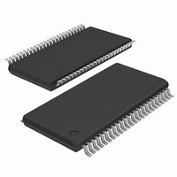
ICS9DB801CGLF IDT, Integrated Device Technology Inc, ICS9DB801CGLF Datasheet

ICS9DB801CGLF
Specifications of ICS9DB801CGLF
Available stocks
Related parts for ICS9DB801CGLF
ICS9DB801CGLF Summary of contents
Page 1
Eight Output Differential Buffer for PCI Express (50-200MHz) Description The 9DB801C is a DB800 Version 2.0 Yellow Cover part with PCI Express support. It can be used embedded systems to provide outputs that have low cycle-to-cycle jitter ...
Page 2
ICS9DB801C Eight Output Differential Buffer for PCI Express (50-200MHz) Pin Configuration SRC_DIV# 1 VDD 2 GND 3 SRC_IN 4 SRC_IN# 5 OE_0 6 OE_3 7 DIF_0 8 DIF_0# 9 GND 10 VDD 11 DIF_1 12 DIF_1# 13 OE_1 14 OE_2 ...
Page 3
ICS9DB801C Eight Output Differential Buffer for PCI Express (50-200MHz) Pin Description for OE_INV = 0 PIN # PIN NAME PIN TYPE 1 SRC_DIV# INPUT 2 VDD POWER 3 GND POWER 4 SRC_IN INPUT 5 SRC_IN# INPUT 6 OE_0 INPUT 7 ...
Page 4
ICS9DB801C Eight Output Differential Buffer for PCI Express (50-200MHz) Pin Description for OE_INV = 0 PIN # PIN NAME PIN TYPE 25 GND POWER 26 PD# INPUT 27 SRC_STOP# INPUT 28 HIGH_BW# INPUT 29 DIF_4# OUTPUT 30 DIF_4 OUTPUT 31 ...
Page 5
ICS9DB801C Eight Output Differential Buffer for PCI Express (50-200MHz) Pin Description for OE_INV = 1 PIN # PIN NAME PIN TYPE 1 SRC_DIV# INPUT 2 VDD POWER Power supply, nominal 3.3V 3 GND POWER Ground pin. 4 SRC_IN INPUT 5 ...
Page 6
ICS9DB801C Eight Output Differential Buffer for PCI Express (50-200MHz) Pin Description for OE_INV = 1 PIN # PIN NAME PIN TYPE 25 GND PWR SRC_STOP IN 28 HIGH_BW DIF_4# OUT 30 DIF_4 OUT 31 ...
Page 7
ICS9DB801C Eight Output Differential Buffer for PCI Express (50-200MHz) Absolute Max Symbol Parameter VDD_A 3.3V Core Supply Voltage VDD_In 3.3V Logic Supply Voltage V Input Low Voltage IL V Input High Voltage IH Ts Storage Temperature Tambient Ambient Operating Temp ...
Page 8
ICS9DB801C Eight Output Differential Buffer for PCI Express (50-200MHz) Electrical Characteristics - Clock Input Parameters 70°C; Supply Voltage PARAMETER SYMBOL Differential Input High Voltage V IHDIF Differential Input Low Voltage V ILDIF Input ...
Page 9
ICS9DB801C Eight Output Differential Buffer for PCI Express (50-200MHz) Common Recommendations for Differential Routing L1 length, route as non-coupled 50ohm trace L2 length, route as non-coupled 50ohm trace L3 length, route as non-coupled 50ohm trace Rs Rt Down Device Differential ...
Page 10
ICS9DB801C Eight Output Differential Buffer for PCI Express (50-200MHz) Alternative Termination for LVDS and other Common Differential Signals (figure 3) Vdiff Vp-p Vcm 0.45v 0.22v 1.08 0.58 0.28 0.6 0.80 0.40 0.6 0.60 0.3 1.2 R1a = R1b = R1 ...
Page 11
ICS9DB801C Eight Output Differential Buffer for PCI Express (50-200MHz) General SMBus serial interface information for the ICS9DB801C How to Write: • Controller (host) sends a start bit. • Controller (host) sends the write address DC • ICS clock will acknowledge ...
Page 12
ICS9DB801C Eight Output Differential Buffer for PCI Express (50-200MHz) SMBus Table: Frequency Select Register, READ/WRITE ADDRESS (DC/DD) Byte 0 Pin # - PD_Mode Bit 7 - STOP_Mode Bit 6 Bit 5 - Reserved - Reserved Bit 4 - Reserved Bit ...
Page 13
ICS9DB801C Eight Output Differential Buffer for PCI Express (50-200MHz) SMBus Table: Vendor & Revision ID Register Byte 4 Pin # - Bit 7 - Bit 6 - Bit 5 - Bit 4 - Bit 3 Bit 2 - Bit 1 ...
Page 14
ICS9DB801C Eight Output Differential Buffer for PCI Express (50-200MHz) Note: Polarities in timing diagrams are shown OE_INV = 0. They are similar to OE_INV = 1. PD#, Power Down The PD# pin cleanly shuts off all clocks and places the ...
Page 15
ICS9DB801C Eight Output Differential Buffer for PCI Express (50-200MHz) SRC_STOP# The SRC_STOP# signal is an active-low asynchronous input that cleanly stops and starts the DIF outputs. A valid clock must be present on SRC_IN for this input to work properly. ...
Page 16
ICS9DB801C Eight Output Differential Buffer for PCI Express (50-200MHz) SRC_STOP_3 (SRC_Stop = Driven Tristate) SRC_Stop# PWRDWN# DIF (Free Running) DIF# (Free Running) DIF (Stoppable) DIF# (Stoppable) SRC_STOP_4 (SRC_Stop = Tristate Tristate) SRC_Stop# PWRDWN# DIF (Free Running) ...
Page 17
ICS9DB801C Eight Output Differential Buffer for PCI Express (50-200MHz INDEX INDEX AREA AREA 45° Ordering Information 9DB801CFLFT Example: XXXX IDT TM /ICS TM Eight ...
Page 18
ICS9DB801C Eight Output Differential Buffer for PCI Express (50-200MHz INDEX INDEX AREA AREA Ordering Information 9DB801CGLFT Example: XXXX IDT TM /ICS TM Eight ...
Page 19
ICS9DB801C Eight Output Differential Buffer for PCI Express (50-200MHz) Revision History Rev. Issue Date Description A 4/8/2005 Release to Final 1. Added Polarity Table. 2. Updated Electrical Characteristics. 3. Updated LF Ordering Information from "Annealed Lead Free" 9/7/2006 ...


