CY29947AXC Cypress Semiconductor Corp, CY29947AXC Datasheet
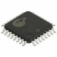
IC CLK BUFF 1:9 200MHZ 32TQFP

CY29947AXC

Manufacturer Part Number
CY29947AXC
Description
IC CLK BUFF 1:9 200MHZ 32TQFP
Manufacturer
Cypress Semiconductor Corp
Type
Fanout Buffer (Distribution), Multiplexerr
Datasheet

Specifications of CY29947AXC

Package / Case
32-TQFP
Number Of Circuits
1
Ratio - Input:output
2:9
Differential - Input:output
Yes/No
Input
LVCMOS, LVTTL
Output
LVCMOS, LVTTL
Frequency - Max
200MHz
Voltage - Supply
2.375 V ~ 3.63 V
Operating Temperature
0°C ~ 70°C
Mounting Type
Surface Mount
Frequency-max
200MHz
Minimum Operating Temperature
0 C
Mounting Style
SMD/SMT
Multiply / Divide Factor
1:9
Number Of Clock Inputs
2
Output Logic Level
LVCMOS, LVTTL
Supply Voltage (max)
3.63 V
Supply Voltage (min)
2.375 V
Maximum Operating Temperature
+ 70 C
Lead Free Status / RoHS Status
Lead free / RoHS Compliant
Lead Free Status / RoHS Status
Lead free / RoHS Compliant, Lead free / RoHS Compliant
Other names
428-2235
CY29947AXC

Available stocks

Company
Part Number
Manufacturer
Quantity
Price
Part Number:
CY29947AXC
Manufacturer:
Renesas
Quantity:
29
Part Number:
CY29947AXC
Manufacturer:
Cypress Semiconductor Corp
Quantity:
10 000
Part Number:
CY29947AXCT
Manufacturer:
Cypress Semiconductor Corp
Quantity:
10 000
47
Features
Cypress Semiconductor Corporation
Document #: 38-07287 Rev. *C
• 2.5V or 3.3V operation
• 200-MHz clock support
• LVCMOS-/LVTTL-compatible inputs
• 9 clock outputs: drive up to 18 clock lines
• Synchronous Output Enable
• Output three-state control
• 250 ps max. output-to-output skew
• Pin compatible with MPC947, MPC9447
• Available in Industrial and Commercial temp. range
• 32-pin TQFP package
Block Diagram
TCLK_SEL
SYNC_OE
TCLK0
TCLK1
TS#
0
1
VDD
VDDC
2.5V or 3.3V, 200-MHz, 1:9 Clock Distribution Buffer
3901 North First Street
9
Q0-Q8
Description
The CY29947 is a low-voltage 200-MHz clock distribution buff-
er with the capability to select one of two LVCMOS/LVTTL
compatible clock inputs. The two clock sources can be used
to provide for a test clock as well as the primary system clock.
All other control inputs are LVCMOS/LVTTL compatible. The 9
outputs are LVCMOS or LVTTL compatible and can drive 50
series or parallel terminated transmission lines.For series ter-
minated transmission lines, each output can drive one or two
traces giving the device an effective fanout of 1:18. The out-
puts can also be three-stated via the three-state input TS#.
Low output-to-output skews make the CY29947 an ideal clock
distribution buffer for nested clock trees in the most demand-
ing of synchronous systems.
The CY29947 also provides a synchronous output enable in-
put for enabling or disabling the output clocks. Since this input
is internally synchronized to the input clock, potential output
glitching or runt pulse generation is eliminated.
Pin Configuration
TCLK_SEL
SYNC_OE
TCLK0
TCLK1
VDD
VSS
VSS
TS#
San Jose
1
2
3
4
5
6
7
8
CY29947
CA 95134
Revised December 22, 2002
24
23
22
21
20
19
18
17
VSS
Q3
VDDC
Q4
VSS
Q5
VDDC
VSS
CY29947
408-943-2600
[+] Feedback

Related parts for CY29947AXC

CY29947AXC Summary of contents

Page 1

... TCLK1 TCLK_SEL SYNC_OE TS# Cypress Semiconductor Corporation Document #: 38-07287 Rev. *C 2.5V or 3.3V, 200-MHz, 1:9 Clock Distribution Buffer Description The CY29947 is a low-voltage 200-MHz clock distribution buff- er with the capability to select one of two LVCMOS/LVTTL compatible clock inputs. The two clock sources can be used to provide for a test clock as well as the primary system clock ...

Page 2

Pin Description Pin Name PWR 3 TCLK0 4 TCLK1 2 TCLK_SEL 11, 13, 15, 19, Q(8:0) VDDC 21, 23, 26, 28 SYNC_OE 6 TS# 10, 14, 18, 22, VDDC 27 VDD 12, ...

Page 3

Maximum Ratings Maximum Input Voltage Relative ............. V SS Maximum Input Voltage Relative to V :............. V DD Storage Temperature: ................................ –65° 150°C Operating Temperature: ................................ –40°C to +85°C Maximum ESD protection ................................................ 2kV ...

Page 4

AC Parameters : 3.3V ±10% or 2.5V ±5%, Over the specified temperature range DD DDC Parameter Description [6] Fmax Input Frequency [6] Tpd TCLK To Q Delay [6, 7] FoutDC Output Duty Cycle tpZL, tpZH ...

Page 5

Pulse Generator ohm Figure 2. LVCMOS_CLK CY29947 Test Reference for V LVCMOS_CLK Q Figure 3. LVCMOS Propagation Delay (TPD) Test Reference Document #: 38-07287 Rev. *C CY29947 DUT ohm ohm R ...

Page 6

... Document #: 38-07287 Rev. *C © Cypress Semiconductor Corporation, 2002. The information contained herein is subject to change without notice. Cypress Semiconductor Corporation assumes no responsibility for the use of any circuitry other than circuitry embodied in a Cypress Semiconductor product. Nor does it convey or imply any license under patent or other rights. Cypress Semiconductor does not authorize its products for use as critical components in life-support systems where a malfunction or failure may reasonably be expected to result in significant injury to the user ...

Page 7

Revision History Document Title: CY29947 2.5V or 3.3V, 200-MHz, 1:9 Clock Distribution Buffer Document Number: 38-07287 Issue REV. ECN NO. Date Change ** 111098 02/07/02 *A 116781 08/14/02 *B 118462 09/09/02 *C 122879 12/22/02 Document #: 38-07287 Rev. *C Orig. ...

Related keywords