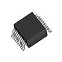
IDT49FCT805PYGI IDT, Integrated Device Technology Inc, IDT49FCT805PYGI Datasheet - Page 2

IDT49FCT805PYGI
Manufacturer Part Number
IDT49FCT805PYGI
Description
IC BUFFER/CLOCK DRIVER 20-SSOP
Manufacturer
IDT, Integrated Device Technology Inc
Series
49FCTr
Type
Fanout Buffer (Distribution)r
Datasheet
1.IDT49FCT805APYG.pdf
(7 pages)
Specifications of IDT49FCT805PYGI
Number Of Circuits
2
Ratio - Input:output
1:5
Differential - Input:output
No/No
Input
LVTTL
Output
CMOS
Frequency - Max
166MHz
Voltage - Supply
4.75 V ~ 5.25 V
Operating Temperature
-40°C ~ 85°C
Mounting Type
Surface Mount
Package / Case
20-SSOP
Frequency-max
166MHz
Number Of Outputs
10
Operating Supply Voltage (max)
5.25V
Operating Temp Range
-40C to 85C
Propagation Delay Time
8ns
Operating Supply Voltage (min)
4.75V
Mounting
Surface Mount
Pin Count
20
Operating Supply Voltage (typ)
5V
Package Type
SSOP
Input Frequency
80MHz
Operating Temperature Classification
Industrial
Lead Free Status / RoHS Status
Lead free / RoHS Compliant
Other names
49FCT805PYGI
PIN CONFIGURATION
NOTE:
1. Pin 8 is not internally connected on devices with a "K" prefix in the date code. On older
devices, pin 8 is internally connected to GND. To insure compatibility with all products,
pin 8 should be connected to GND at the board level.
IDT49FCT805/A
FAST CMOS BUFFER/CLOCK DRIVER
GND
V
OE
NC
OA
OA
OA
OA
OA
CCA
IN
A
A
A
4
1
2
3
5
(1)
1
10
2
3
4
5
6
7
8
9
SOIC/ SSOP
TOP VIEW
20
19
16
15
12
18
17
14
11
13
IN
OB
OB
OB
GND
OB
OB
MON
OE
V
CC
B
2
1
3
4
5
B
B
2
ABSOLUTE MAXIMUM RATINGS
NOTES:
1. Stresses greater than those listed under ABSOLUTE MAXIMUM RATINGS may cause
2. Input and V
3. Output and I/O terminals.
CAPACITANCE (T
NOTE:
1. This parameter is measured at characterization but not tested.
PIN DESCRIPTION
FUNCTION TABLE
NOTE:
1. H = HIGH
Symbol
Symbol
V
V
C
TERM (2)
TERM (3)
T
permanent damage to the device. This is a stress rating only and functional operation
of the device at these or any other conditions above those indicated in the operational
sections of this specification is not implied. Exposure to absolute maximum rating
conditions for extended periods may affect reliability.
C
L = LOW
Z = High-Impedance
I
OUT
OE
OUT
STG
IN
Pin Names
OAn, OBn
OE
IN
A
MON
, OE
H
H
COMMERCIAL AND INDUSTRIAL TEMPERATURE RANGE
A
L
L
A
, OE
, IN
B
B
CC
Description
Terminal Voltage with Respect to GND
Terminal Voltage with Respect to GND
Storage Temperature
DC Output Current
Parameter
Input Capacitance
Output Capacitance
B
Inputs
terminals.
(1)
3-State Output Enable Inputs (Active LOW)
Clock Inputs
Clock Outputs
Monitor Output
IN
A
H
H
, IN
L
L
B
A
= +25
Conditions
(1)
V
V
OUT
IN
Description
= 0V
= 0V
O
OAn, OBn
C, f = 1.0MHz)
H
L
Z
Z
Typ.
4.5
5.5
–0.5 to V
–65 to +150
Outputs
–60 to +60
–0.5 to +7
Max
CC
Max.
(1)
6
8
+0.5
MON
H
H
L
L
Unit
pF
pF
Unit
mA
°C
V
V


